Angular Resolved Photoluminescence and Electroluminescence of light emitting materials

OLEDs and quantum dot (QD) enhanced LCDs are the key technologies for today‘s best-in-class displays for both mobile and TV applications. LEDs, or Organic Light Emitting Diodes, are renowned for providing superior contrast ratios and image quality compared to their LCD (Liquid Crystal Display) counterparts. This has made them the go-to choice for a wide range of applications, including smartphone displays, high-definition TVs, and automotive tail lights. The ability of OLEDs to produce true black colors by turning off individual pixels contributes significantly to their exceptional visual performance.
The display industry has a constant need to characterize light-emitting OLED and quantum dot materials in its constant drive for brighter, more colorful, sharper, and more efficient displays. Especially, it is crucial to address and enhance their luminous efficiency, commonly referred to as the lumen/watt ratio. Improving this ratio ensures that OLEDs generate more light output per unit of electrical power consumed, ultimately leading to increased energy efficiency and extended device lifetimes. All of these display characteristics are strongly influenced by the orientation, position, and spectrum of the light-emitting species inside the device stack.
Tuning these material and device parameters is one of the most promising approaches to enhancing the efficiency of state-of-the-art OLEDs and quantum dots.
What is determining the OLED efficiency
Figure 1 is a schematic illustration of a planar OLED showing that only a small fraction of light is emitted to the air outside the device due to optical losses (left side of the illustration). These losses are identified as Waveguide modes and Emission to substrate (or Substrate modes) which limit the outcoupling efficiency. Both losses are caused by a mismatch in the refractive indexes between emitter and electrode layers, in the case of the Waveguide modes, or the substrate and the air, in the case of the Emission to substrate. The mismatch causes internal reflection of the emitted light that will escape from the edges or be absorbed into the device. As an example, optical losses Substrate modes can be minimized with the application of an index-matched Glass prism (right side of the image).

Fig. 1 Schematic representation of ray propagaion in a planar OLED. The green and red arrows indicate optical losses happening due to internal reflection waveguide modes and the substrate, respectively. Internal quantum efficiency (IQE) is the emission from the active emitting layer and the external quantum efficiency (EQE) is the emission of the full device within the escape cone. [Brü12]
To discuss light-outcoupling optimization, we must first introduce two figures of merit: internal quantum efficiency (IQE) and external quantum efficiency (EQE). IQE refers to the bare active material's emission, while EQE quantifies the full device's light emission within the escape cone, which depends on the device structure and the refractive index of the layers. Despite achieving an IQE of 100%, the best OLED devices have an EQE of less than 30%, indicating that more than 70% of the generated light is not emitted outside the device.
The EQE can be written in various equivalent forms:


Regardless of their complexity, it can be expressed as the product of two factors:
the number of injected charges that form light-emitting excitons (IQE);
the amount of light effectively emitted, or light outcoupling efficiency (ηout).
It follows that the simplest form to express the EQE is:

In this way, it is easy to see that if we already reach an IQE of 100%, then we need to focus on the light outcoupling efficiency (ηout) to increase the EQE of OLEDs.
Light Outcoupling Efficiency in Organic Emitters
Organic emitters, unlike inorganic semiconductors, are made of molecules that act as light-emitting dipoles.
The orientation of these dipoles has a direct impact on the optical outcoupling efficiency, with emission perpendicular to the substrate being strongest for horizontally aligned dipoles and zero for vertically aligned dipoles


Fig 2. Schematic representation of the dipole’s orientation with respect to the device substrate (left). Simulated data of angle-dependent photoluminescence for dipoles with horizontal, isotropic and vertical orientation with respect to the substrate of the light-emitting device (right). The 0° angle indicates emission perpendicular to the device substrate
The orientation of the molecules and their dipoles can be influenced by factors such as temperature, deposition method, and molecular structure. For horizontal orientation, one should consider: low deposition temperatures, vacuum deposition over solution-processing, and molecules with a high aspect ratio.
Measuring Dipole Orientation with Angle-Dependent Photoluminescence
Angle-dependent photoluminescence is a reliable method for determining the orientation of dipoles. Tools like Phelos are designed to characterize light-emitting devices and thin films at various emission and polarization angles. The sample is mounted on a rotating half-cylindrical lens while excited with LED light and the emission is recorded by a detector equipped with a polarizer.

Fig 3. Diagram showing an LED sample mounted on a rotating half-cylindrical lens while excited with LED light, while the emission is recorded by a detector equipped with a polarizer.
The emitted light is s- or p- polarized, depending on if its electric field is perpendicular or horizontal to the plane of incidence, respectively. When the molecules are horizontally oriented, the p-polarized emission is strongest and perpendicular to the substrate.


Fig 4. Diagram showing how emitted light is s- or p- polarized, depending on if its electric field is perpendicular or horizontal to the plane of incidence, respectively. (Right) The orientation of the dipoles is determining the efficiency of the OLED.

The orientation of the dipoles is quantified with ϴ, which is the average orientation of an ensemble of radiating electrical dipoles with dipole moment p. (see equation on the right)
With this definition, an orientation of 0 represents a fully horizontal, 1 a fully vertical and 0.33 an isotropic oriented ensemble.
Example: Dipole Orientation in Oriented CdSe Nanoplatelets and Perovskite Quantum Dots
Angular resolved PL and EL are popular methods to characterize light-emitting materials and OLEDs.

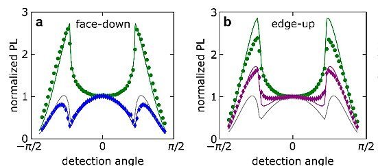
Fig 5: illustration of face down and edge-up orientation of CdSe nanoplateletes (left). Angle-resolved PL of a face-down (a) and edge-up (b) nanoplatelets assembly. Dotted lines are the experimental measurements and the cotinous line the fitting of the measurement. The green and blue/purple colors indicate the s and p polarized light radiation, respectively (right).
By applying a similar analysis to inorganic systems, we can gain insights into the intensity of light emission. For example, Momper et al. [MOM20] used angle-dependent photoluminescence measurements with Phelos on CdSe nanoplatelets to study the influence of light emission intensity. Face-down platelets exhibit lower p-polarized light intensity than edge-up nanoplatelets. (Figure 5)
Similarly can be done for perovskite-based quantum dot LEDs. Kumar et al. [Kum22] tailored the growth of perovskite nanocrystals to obtain a preferentially horizontal orientation of the dipoles to increase the light outcoupling. With angle-resolved PL intensity measurements, they could quantify the ratio of horizontal dipoles. An enhanced ratio of horizontal dipoles leads to the disappearance of the emission intensity at 41° and reduces the emission for viewing angles bigger than 41°. (Figure 6)

Fig. 6: experimentally characterized PL intensity (dotted line) and calculated PL intensity for various dipole orientations (ΘH = 0.67, 0.72, 0.91, 1) as function of viewing angle.
How to Perform an Angular Resolved PL Measurement
The combination of the characterization tool Phelos and the simulation software Setfos can be used to study light-emitting materials by extracting important parameters, such as the orientation of the dipoles and the width of the emission zone. This allows us to further optimize OLEDs that are using these materials, to reach higher External Quantum Efficiency (EQE).
Here, as an example, we are showing how to characterize a thin film of a green organic emitter deposited on a glass substrate with the angular-resolved photoluminescence (PL) setup, Phelos.
This gonio-spectrometer measures the full emission spectrum of OLEDs and QD down-conversion films as a function of the emission angle and light polarization. The angular spectrum and polarization are fingerprints of the emitter molecules’ orientation and of the position inside the emitting layer, where electrons and holes recombine and generate light. In combination with built-in optical simulations, from a single emitting layer up to the full OLED stack, the angular characteristics, therefore, allow for reliable and accurate extraction of these key quantities for OLED and QD material optimization.
Angular EL and PL analyses have significant advantages over traditional approaches to characterize the optical transition dipoles, like variable-angle spectroscopic ellipsometry (VASE), because the method is not limited to pure emitter films: From the angular photoluminescence characteristics, the dipole orientation can be precisely analyzed even if the emitters are embedded in a host matrix.
We measured the p-polarized and s-polarized emission spectra of this material over a wide range of angles by exciting at 275 nm (or at 405 nm). Figure 6 shows the s-polarized PL spectrum recorded a 0 deg, as an example. Phelos can also perform angular electroluminescence (EL) measurements to characterize a full OLED stack.

Figure 6: PL measurements with Phelos. The integrated driving software is capable of both data collection and analysis.
With the integrated software Characterization Suite, we can define the device and the experiment to start the measurement:
We define the experimental setting, as shown in Figure 7 (defined in the tab "Measurement Procedure").
In the tab "Acquire and Manage Data" we create a new device and select Measure Device to start the measurement.

Figure 7: PL experimental settings in the Characterization Suite Software
After the measurement, we export all measured data to Setfos to run a fitting algorithm :
We open the export dialogue from the menu Phelos => Export Phelos Meas. for Setfos
We select a device and a measurement and then click on the Export button
Data Fitting with Setfos for Advanced Parameter Extraction
To perform the data fitting with Setfos, we need the emission module and the optimization mode. The Emission Module uses the dipole emission model and can be used to model several properties of a light-emitting material and of a Light-Emitting Diode (LED). In this particular example, we will couple Setfos with Phelos to determine the orientation of the dipoles in our light-emitting film.
Figure 8 shows the Setfos GUI with highlighted:
a section (red line) to define the layer structure, such as the layer thickness, the nk files of layers.
a section (green line) to define the wavelength range, the angle of the emission, and the emission mode (spectral, dissipation power analysis, mode analysis).
a section (yellow line) to define the emitting layer, emission spectrum, dipole distribution, position, and orientation.

Figure 8: Setfos Graphical User Interface (GUI)
Then, we have to define the target of the fitting ( Simulation settings => Optimize settings => Targets). We use Spectral Sweep as target mode, and the s- and p- experimental spectral intensities obtained by Phelos. During the fitting, we can also easily extract the luminescence spectrum (select extract luminescence spectrum below the target definition, and choose white instead of file for luminance in the main window).

Figure 9: Definition of the fitting parameters/targets
We also have to choose the optimization parameters, such as the emission layer thickness, the dipole position, orientation, and the emission intensity. This is done with Simulation settings => Optimize settings => Parameters.
We need to define reasonable min and max values of the fitting parameters, in order to find the global minimum of the error function in the optimization.
Finally, we need to define the method to get the best starting point for each parameter.
InitVal: the optimization will start at the given value
Elements: Setfos will take linearly N points between min and max to choose the best starting point.
Elements log: is in the same principle as the method elements by taking points logarithmically.
Delta: will take a point with a given step.
Results and comparison between measurement and simulation
After the optimization, we obtain values for all optimization parameters.

Figure 10: Results obtained by fitting the experimental results with Setfos.
We can compare the simulated radiance vs angle with the experimental data. Also, the simulated spectra can be compared to the experimental data to qualify the simulation results.

Figure 11: Comparison between measured data and fitted data for the radiance and the normalized spectrum
Figure 12 shows the comparison between simulation and experiment at five different angles. We can see that there is a good matching between measurement and simulation for both p- and s-polarization at each angle. This is showing the potential of Setfos to understand the main mechanisms regulating light emission from the organic material.

Figure 12: Comparison between measured data and fitted data for spectrum at different angles
Conclusions
OLED technology offers higher contrast ratios compared to LCD technology. However, the luminous efficiency of OLEDs, or lumen/watt ratio, needs improvement to increase the light output. To achieve this goal it is necessary to increase the light outcoupling efficiency (ηout).
The organic emitters found in OLEDs are constituted by dipoles, which orientation affects ηout with horizontal alignment leading to the highest efficiency. Angle-dependent photoluminescence is an effective method for determining dipole orientation. With Phelos you can perform both angle-dependent photoluminescence and electroluminescence and its coupling with the simulation software Setfos it is a powerful combination for data analysis, parameter extraction, and device modeling.
Ultimately, by tailoring the orientation of organic emitters and comprehensively investigating the factors that impact emission intensity, we can continue to advance OLED technology. Further research and development in this area will contribute to increased energy efficiency, extended device lifetimes.
References
[Kum22] Kumar et al., “Anisotropic nanocrystal superlattices overcoming intrinsic light outcoupling efficiency limit in perovskite quantum dot light-emitting diodes“ Nat. Commun. 2022, 13, 1.
To learn more about angle-dependent measurements, we recommend the following article:
https://www.fluxim.com/fluxim-blog/light-conversion-perovskite-quantum-dots