
Setfos
Simulation Software for Organic and Perovskite Solar Cells, Photodetectors & LEDs
Setfos excels in analyzing and fitting experimental data, providing researchers with valuable insights and trend predictions. Complement your experimental work with Setfos for unmatched accuracy and reliability in data interpretation
Simulation software for optical and electrical modeling of semiconducting devices. Designing LEDs & solar cells based on organic semiconductors, perovskites, and quantum-dots.
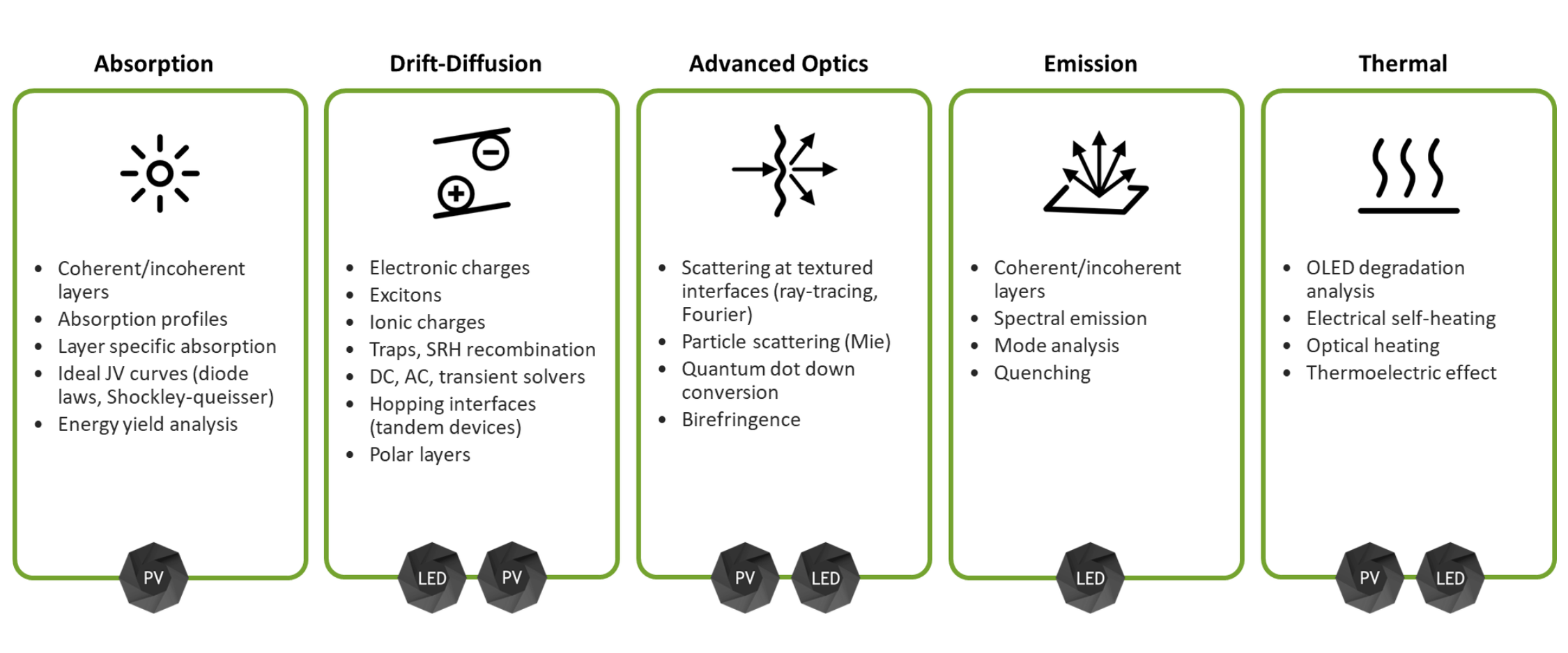
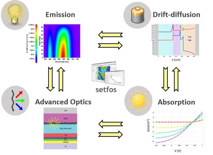
Four different modules to simulate light emission, absorption, scattering, and charge transport.
Multithreading ensures high-speed computation.
Fitting and optimization algorithms are included.
Outstanding track record: 20 years in industry and academia resulting in over 200 scientific publications. Sound materials & device models have been successfully validated by dedicated experiments.
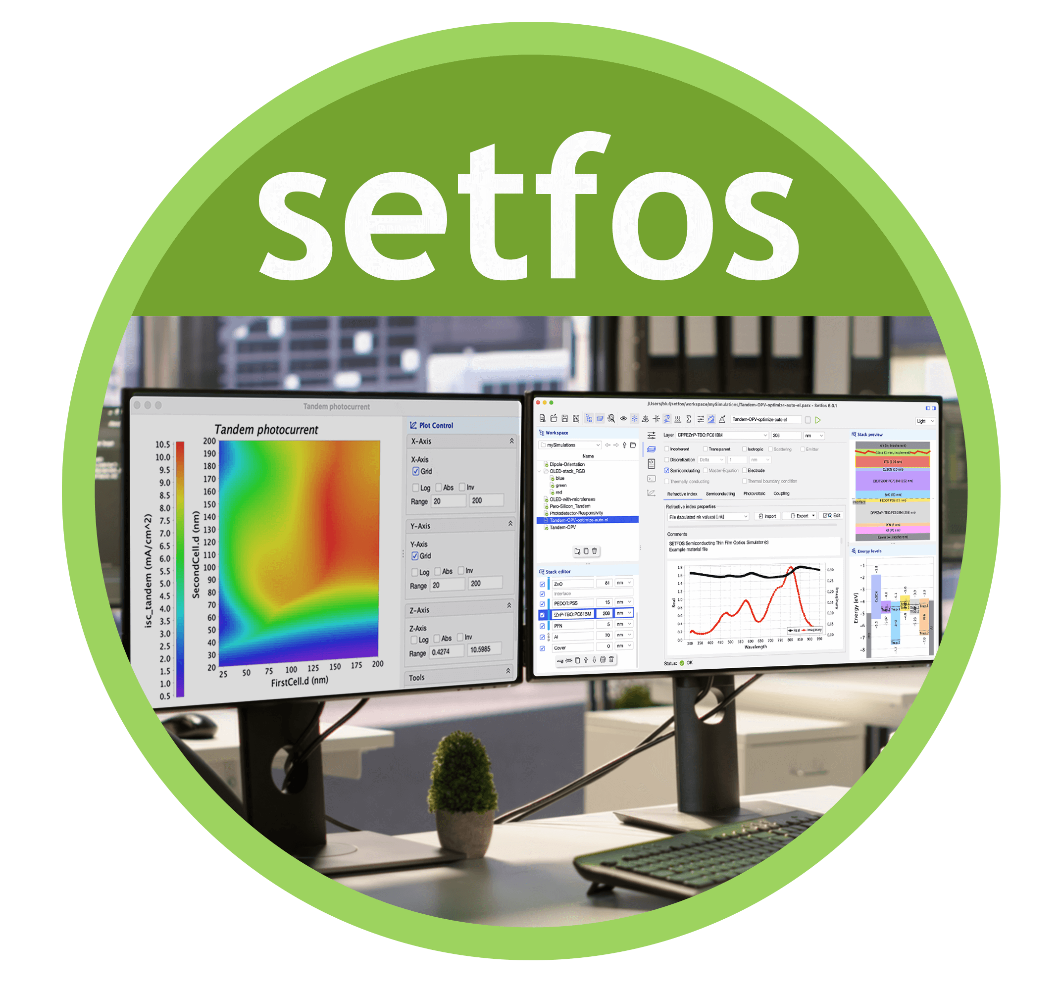
Graphical User Interface
Intuitive access to device structure, material parameters, working files, and simulation output.
Optimization Toolbox to maximize the device efficiency.
Sweep function to analyze the influence of the material parameters on the device efficiency.
Easy access to a library of simulation examples and material property databases.
Key graphs and reports are automatically generated. Multiple simulations can run in parallel.
The graphical user interface (GUI) shows the device design and the results from the simulation in intuitive plots. The results can be exported to a number of different formats. Setfos is fully compatible with Python.
Meet The Setfos Experts
Our team of Setfos experts is dedicated to advancing OLED and solar cell research. With years of experience in the field, they provide unparalleled support and insights to optimize your projects. Whether you're tackling complex simulations or fine-tuning device performance, our experts are here to guide you every step of the way, ensuring precision and innovation in your research endeavors.


Dr. Urs Aeberhard
Dr. Balthasar Blülle

Dr. Sandra Jenatsch

Dr. Davide Moia

Dr. Markus Regnat
Solar Cell Modeling
Easily calculate the short circuit current (Jsc), open-circuit voltage (Voc), and fill factor. Tweak the layer stack and add light scattering layers to enhance light absorption.
Specific for organic, quantum-dots, and perovskite solar cells.
Optimize the device for the AM1.5 (or for specific wavelengths) with the Absorption Module.
Curve fitting & parameter extraction. Understanding the origin of the hysteresis in perovskite solar cells.
AC simulation of transient experiments, as photo-CELIV. Easy to couple with the electrical characterization systems Paios.
Advanced device physics: SRH-recombination, excitons, ...
Designing anti-reflection coatings or transparent solar cells.


Try PV data fitting in Setfos
Fit perovskite JV and EQE from measurement data.
How to Simulate a Perovskite Solar Cell with Setfos
Watch this video tutorial by Dr. Urs Aeberhard to learn how to simulate a perovskite solar cell using Setfos.
Although demonstrated with an organic example, the workflow and drift-diffusion modeling steps are identical for perovskites.
Perovskite Solar Cell Simulation Tutorial with Setfos
Workflow Overview
- Step 1: Define layer stack (absorber, transport, electrodes)
- Step 2: Set optical properties (import n/k data)
- Step 3: Choose simulation type (optical, electrical, full)
- Step 4: Configure drift-diffusion solver (recombination, traps, contacts)
- Step 5: Run simulation & extract J‑V curve
- Step 6: Analyze and export results (performance, plots, data)
““In this tutorial, I show how to set up and run Setfos simulations of organic solar cells. While the example is organic, the exact same process applies to perovskite devices using the drift-diffusion model, Shockley-Read-Hall recombination, and full opto-electronic coupling.””
Frequently Asked Questions
Q1: How do I simulate a perovskite solar cell step by step?
Using Setfos, you define the layer stack (e.g. perovskite absorber, transport layers), import optical data (n and k values), configure electrical parameters (mobility, recombination), and run a drift-diffusion simulation to extract JV curves and efficiency.
Q2: What simulation model is used for perovskite solar cells in Setfos?
Setfos uses a coupled optical and electrical model. The optical simulation solves Maxwell’s equations to compute generation profiles, while the electrical module solves the drift-diffusion equations to simulate charge transport and recombination.
Q3: Can Setfos simulate perovskite solar cells under different lighting conditions?
Yes. You can simulate illumination with AM1.5G, indoor LED spectra, or custom light sources. Setfos supports both high- and low-intensity scenarios, ideal for indoor PV or tandem device analysis.
Q4: Do I need experimental data to simulate perovskite solar cells?
Not necessarily. Setfos includes a database of common materials and optical constants. However, importing your own n/k and mobility data improves accuracy and matches experimental results more closely.
Q5: Is Setfos suitable for both single-junction and tandem perovskite solar cells?
Yes. Setfos supports single-junction perovskite devices and can also simulate complex multi-junction architectures like perovskite-silicon tandems, including recombination layers and optical interference.
OLED Modeling
Setfos simulates OLEDs from charge injection to light extraction. The graphical user interface makes it easy to analyze and improve your devices. Modeling OLEDs from the material selection to the definition of the most efficient stack.
Modeling charge transport and recombination with the Drift Diffusion module.
Analyze optical emission spectra and wave-guided mode contributions with the Emission Module
Design out-coupling layers for efficiency and color stability.
Design scattering layers to enhance the light out-coupling with the Advanced Optics Module
Advanced device physics: quenching, excitons, traps, doping, AC & transient responses, ...
How to Simulate an OLED with Setfos
Learn how to simulate OLED devices using Setfos, Fluxim’s simulation tool for opto-electronic modeling. In this tutorial, Dr. Urs Aeberhard walks through defining the layer stack, modeling charge injection and recombination, and simulating optical outcoupling using Setfos. This process helps OLED researchers analyze efficiency, spectra, and current-voltage characteristics.
OLED Simulation Workflow in Setfos
- 00:15 – Define OLED layer stack (HTL, EML, ETL, electrodes)
- 01:05 – Import optical constants (n/k data)
- 02:30 – Set electrical models (mobility, recombination, injection layers)
- 03:45 – Run drift-diffusion + optical emission
- 05:10 – Analyze J–V, EQE, emission spectra, and out‑coupling efficiency
OLED Simulation FAQ
Q: Can Setfos simulate light extraction in OLED devices?
A: Yes. Setfos uses dipole emission and advanced optics modules to model micro-cavity effects, emission patterns, and out-coupling efficiency.
Q: What electrical models does Setfos support for OLEDs?
A: Drift‑diffusion with charge injection, mobility, exciton recombination, and quenching. Plus field‑dependent and transient models.
Q: Is Setfos used in academic OLED R&D?
A: Absolutely. It’s employed by research groups worldwide in academia and industry for emission spectra, efficiency, waveguide mode analysis, and device lifetime studies.
Q: Can Setfos simulate exciton behavior?
A: Yes. It can model exciton generation, migration, quenching, and Purcell effects using its emission module.
Q: Can it handle tandem or stacked OLEDs?
A: Yes, complex multi-layer and tandem structures with optical interference and out-coupling layers are fully supported.
Parameter Sweep and Device Optimization
Sweep parameters to understand their effect on the device properties.
Setfos contains a powerful optimization engine that can be used to find the device layout that gives the highest efficiency automatically.
You can fit parameters to experimental data from DC, AC, and transient analyses of solar cells and LEDs.
You can choose between different visualizations of the results to easily Light Emission Simulation
Setfos uses the dipole emission model to predict the light emission characteristics of an OLED. Several device properties can be modelled:
Electroluminescence emission pattern.
Micro-cavity effects by thin-film optics.
Photophysical properties such as efficiency, angular colour, and brightness changes.
Excitonic processes in OLEDs by combining optical and electrical simulation.
Waveguided and plasmonic modes, quenching, distribution, and orientation of the emitters.
A number of scientific publications demonstrate the potential of Setfos for OLED modeling.
-
Setfos calculates the optical parameters of an OLED by taking into account the full micro-cavity behavior. This includes but it is not limited to:
CIE xy color coordinates.
Brightness (cd/m2).
Luminous Efficacy (Lm/W).
Luminous Current Efficiency (lm/A).
Correlated Color Temperature (CCT).
Color Rendering Index (CRI).
Reflectance, transmittance, and absorbance.
-
Setfos Mode Analysis can analyze light emission through the different emission channels of an OLED. The emitted light either escapes to the far field or is waveguided inside the OLED layers. Without outcoupling structures, only the light emitted inside the escape cone is visible to the observer.Mode analysis simulation calculates the contribution of the different optical modes to the total emitted power:
Air modes escaping to the outside.
Substrate modes waveguided in the carrier substrate.
Organic modes waveguided in the organic semiconductor stack.
Plasmon modes coupled to the metal electrodes.
Non-radiative quenching losses.
Modes can be inspected across the spectrum or summarized, considering the emitter's spectral distribution.
-
An OLED design is not limited to the stack of organic semiconductors. There are also colour filters and anti-reflection layers that are used to obtain a higher lighting efficiency.
Setfos calculates the colour, angular variation, and polarization of the whole OLED stack, including coherent optics in the microcavity and coatings incoherently coupled through the substrate.
-
Powerful fitting algorithms let you extract material parameters from measurement data. The optimization routines find the optimal combination of several variables.
Fitting of the emission zone in a complex multilayer stack. Find the spatial distribution of the emitting molecules.
Determine the optical n & k values from reflectance and transmittance measurements. This uses the Sellmeier, Tauc-Lorentz, or Cauchy model.
Use spectral measurements to determine the intrinsic spectrum of an emitter/host system.
Determine the orientation of the emitter dipole by polarized spectroscopy or angular measurements.
Position-dependent Purcell Effect from the data obtained by experiments or simulations.
SETFOS FEATURES


Setfos Videos

T R I A L E V A L U A T I O N