EQE optimization For a Top-Emitting OLED
The external quantum efficiency (EQE) describes the number of outcoupled photons per injected charge and is thus a key figure of merit for an emissive device. It can be divided into 4 factors: charge balance, singlet-triplet factor, radiative quantum efficiency, and light outcoupling efficiency:

We will here focus on the last parameter, the outcoupling efficiency. In an OLED stack, only part of the generated light can escape the device, which can be mainly attributed to the high refractive index of the organic layer. Most of the light is lost to three loss channels (for a top-emitting OLED):
guided modes (total internal reflection)
absorption losses (absorption in layers and at electrodes interface)
surface-plasmon-polariton (evanescent coupling mode)
The importance of these loss channels is influenced by various parameters. Some of them can be controlled or at least adjusted while others can only be monitored. While the basics for outcoupling efficiency can be understood from ray optical considerations, the situation can easily get more complicated when real TEOLED stacks are considered. This makes the use of simulation-assisted optimizations inevitable.
This tutorial is showing how to use Simulation and Characterization to improve the EQE of an OLED. You will be learning how to:
Understand why the angular spectrometer Phelos and the simulation software Setfos should be used to determine the emitter orientation, emitter position, and emission spectrum.
Use Setfos to optimize the EQE for HTL, ETL, and electrode material, the dipole orientation, and position should be known from Setfos fitting to optimize layer thicknesses.
Optimize the outcoupling efficiency by changing layers material, emitter properties, and electrode material.
If you are interested in check the capability of Setfos or Phelos, you can get in contact with us
1. A simplified picture to outcoupling efficiency
In a simplified picture of a bottom-emitting OLED, the losses due to guided modes that limit the outcoupling efficiency can be understood from simple ray-optical considerations. For the case of a bottom-emitting OLED (Figure 1) light from the emitter has to go through the transparent ITO electrode and the glass substrate to escape the device. As the organic layer has a high refractive index of about 1.8, much higher than the glass (about 1.5) and air (n=1), there are two angles of total internal reflections in a bottom-emitting device. Light can escape the device only if it is emitted within the escape cone which is defined by the materials refractive index contrast. The internal angle of the emitter is defined by the dipole orientation. This simple consideration already motivates why we need to know and ideally control these parameters.
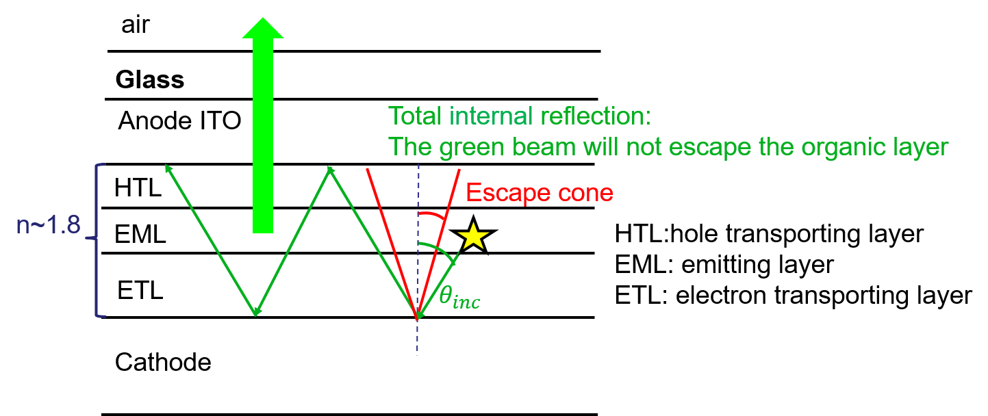
Figure 1: Simplified bottom emitting OLED.
In a real OLED, we also need to consider absorbing hole and electron transporting materials, refractive index dispersions, absorbing electrode materials, and many more effects. The simplified picture from above cannot capture these effects and the use of device simulations becomes necessary.
To simulate the light extraction efficiency of our device, we have to know some properties of the OLED, such as the layer thicknesses and their refractive indices. Moreover, we need to know some quantities from the emitter, namely their position and distribution within the EML, the orientation of the emissive molecules, and the intrinsic emission spectrum. The combination of Phelos and Setfos can help us get this information. If you want to know more about how to determine this topic, please visit our dedicated blog post.
2. Top-emitting OLEDs
In contrast to bottom-emitting OLEDs, TEOLEDs are usually composed of two highly reflecting electrodes (see Figure 2) which are creating multiple optical resonances. This strong cavity allows obtaining a well-defined, narrow emission spectrum in forward direction which is key for display applications. Unfortunately, such strong cavity OLEDs are often prone to angular color shifts and require precise control of each layer thickness. Such thickness optimization and tolerance analysis in order to maximize the EQE and analyze the angular color shift are key applications of Setfos.

Figure 2: Reference stack, top-emitting OLED. Implementation of the structure in the simulation software Setfos.
Figure 2 shows a typical but simple stack of materials forming a top-emitting OLED. Besides the organic transport and emission layer and the two electrodes, top-emitting OLED usually include a capping layer (CPL). This external layer also used to increase the outcoupling efficiency by tuning the CPL thickness. Moreover, the CPL thickness directly influences the emitted color at different angles, as shown in Figure 3.

Figure 3: Impact of the CPL layer
In this tutorial, we will change different material parameters in Setfos to see their impact on the outcoupling efficiency of the OLED. We use mode analysis as emission mode in Setfos to analyze in detail the different loss channel contributions. This will allow optimizing the device solely in the simulation without the need for time- and material-consuming experiments.
For each case in this study, we optimize the outcoupling efficiency firstly with ETL and HTL thicknesses and then with CPL thickness. This optimization step can be done automatically in Setfos.
3. Effect of the layer refractive index
According to a publication by Salehi et al. ("Manipulating refractive index in organic light-emitting diodes"), the layers’ refractive index can be reduced by pore inclusion using oblique angle deposition leading to increased light extraction efficiency in OLED devices. For the simulation with Setfos, we can use different ETL and HTL materials with different refractive indices to investigate the impact on the outcoupling efficiency.
To do the optimization of extraction efficiency, we use the emission module and the sweep mode. By defining the sweep range, we will get results for each case in the range. Figure 4 shows a plot of the outcoupling efficiency I_OC versus HTL and ETL thicknesses, we can see four maxima. We focus on the first and the second maximum in the following.

Figure 4: Outcoupling efficiency versus ETL and HTL thicknesses
In the next step (not shown here) we also optimized the CPL thickness to further improve the outcoupling efficiency of the first and the second maximum.
Figure 5 depicts simulation results for different cases starting from the reference stack to the stack in which both ETL and HTL have lower refractive index material (see table below). The outcoupling efficiency I_OC is equal to 26% for the first maximum in the reference stack which is here used as a benchmark value.


Figure 5: Mode contribution for ETL and HTL change by material with n~1.65
The following trends can be obtained from the simulations:
By decreasing the refractive index of both ETL and HTL materials from 1.8 to 1.65, we increase the outcoupling efficiency I_OC by 31% (compared to the reference stack) in the first maximum and by 25% in the second maximum.
By decreasing the refractive index, we decrease considerably the guided mode plus evanescent coupling mode (I_GM+EC) by 21% for the first maximum and by 30% for the second maximum.
The absorption losses I_AL increase considerably for the second maximum. This explains - especially for the “low ETL high HTL n” case - why I_OC does not increase significantly although the guided and evanescent modes I_GM+EC decrease considerably.
According to the publication by Salehi et al., "It has been shown that the refractive index of Alq3 can be tuned from 1.75 to 1.2 using OAD (oblique angle deposition)". We can therefore further increase the outcoupling efficiency (up to 150% compared to the reference case ) by using an even lower ETL and HTL refractive index (n=1.2). The question remains whether such low-index material can be produced by the same technique using state-of-the-art, doped transport materials.

Figure 6: Mode contribution with lower ETL and HTL refractive index
In the next step, we investigate the influence of the refractive index of the EML while keeping the reasonable values for ETL and HTL (n=1.65). As evident from Figure 7, the conclusion is not the same as above. A higher refractive index of the EML leads to and improved outcoupling efficiency.

Figure 7: Mode contribution for lower EML refractive index (n_ETL=n_HTL~1.65)
This section demonstrates that there is usually significant room for improvement in EQE if only the refractive index of the transport layers, as well as their thicknesses, are tuned. Record high outcoupling efficiencies of above 40% are achieved without the need for complex light outcoupling structures.
Here we have shown the variations step-by-step in order to illustrate the procedure. Of course, Setfos powerful optimization algorithms allow executing the above tasks automatically in one step.
4. Effect of the dipole distribution
Constructive interference of reflection at the electrodes depends on the wavelength, the incidence angle, layers refractive index, layers thicknesses but also on the dipole distribution and position. We consider the low-n (n=1.65) stack with isotropic emission and with optimized layer thicknesses for dipoles with Dirac distribution at position 0, i.e. at the ETL interface. We now change the relative dipole position from 0 to 1 in steps of 0.1. The I_OC is gradually reduced by 22%. These changes are however only because the thicknesses had been optimized for a maximum I_OC at dipole position 0.

Figure 8: Mode contribution versus dipole position for layer thicknesses optimized for dipole at position 0
If we optimize layer thicknesses for each dipole position, we find that the outcoupling efficiency remains constant (Figure 9).

Figure 9: Mode contribution versus dipole position with optimized layers thickness (the first maximum)
Therefore the dipole distribution and position must be known to optimize the layer thicknesses. We can get this crucial information by combining Phelos measurement with Setfos’ emission zone fitting.
5. Effect of the dipole orientation
Emitters can be regarded as dipoles that emit light in a certain direction. In the following, we will study the impact of dipole orientation on the outcoupling efficiency. Figure 10 shows two cases of dipoles in an EML layer, a perpendicular dipole that emits light inside the plane of the emitting layer and a parallel dipole that emits light mostly into the escape cone. The parallel dipole is therefore desirable for more efficient OLEDs.

Figure 10: Two extreme cases of dipole, the perpendicular one and the parallel one
In Setfos, we quantify dipole orientation by a number between 0 and 1. Hereby 0 means all dipoles are parallel/horizontal and 1 means all dipoles are perpendicular/vertical. We consider the low-n stack with dipole position 0.5 (in the center of the EML) and change the dipole orientation from 0 to 1 by steps of 0.1. For each case, we optimize layer thicknesses for the first maximum. The result (Figure 11) shows that parallel dipoles are most efficient with a small contribution of guided-mode plus evanescent mode because the light is almost completely emitted into the escape cone. Between the parallel dipole and the perpendicular one, the optimized layer thicknesses change considerably from 50 nm to 140 nm. By increasing the layer thickness the coupling of the perpendicular dipole emission with guided and evanescent modes can be reduced.

Figure 11: Mode contribution versus dipole orientation
Emission layers with highly parallel dipole orientation will therefore lead to good outcoupling efficiency. This indicates again that it is very important to know this parameter from independent measurements using Phelos and Setfos fitting. It has been shown by Komino et al. that it is (sometimes) possible to manipulate the dipole orientation by specific fabrication conditions.
6. Effect of the electrode material and thickness
We will now consider the low n stack with Dirac distribution at position 0.5, and this time with dipole orientation equal to 0.18 (the result from the fitting). We change the top and bottom electrode material between silver (Ag) and aluminum (Al) to study the impact of the electrode material. Figure 12 shows the difference in absorption and reflection between the two materials. We notice that silver reflects more and absorbs less than aluminum for wavelengths over 420 nm.

Figure 12: Reflectance (solid lines) and absorbance (dashed lines) of Ag and Al versus wavelength
In Figure 13 we plot the comparison of each mode for four cases in the first and second emission maximum. It shows that silver as a semi-transparent top electrode induces fewer absorption losses compared to aluminum. The bottom electrode material has a smaller effect on the I_OC. When silver is used, the guided and evanescent modes are slightly higher. The best case is therefore achieved with silver as the top electrode and aluminum as the bottom electrode.

Figure 13: Mode contribution for four combinations of electrodes material
We can also see an impact on the top electrode thickness. In Figure 14 we plot the mode contributions for top electrode thicknesses of 20, 10, and 5 nm. There is no big impact on the outcoupling efficiency. This allows us to consider electrical effects first and do not use a too thin electrode in order to achieve sufficient conductivity.
There is no impact on the bottom electrode thickness because it is a very thick layer. Optically, the bottom electrode is like a mirror that reflects light.

Figure 14: Mode contribution for different top electrode thicknesses
In Figure 15 we show a summary of the parameter changes employed in our study to increase the outcoupling efficiency. In the reference stack, we already use Ag as the top electrode. We can demonstrate an increase of the EQE from 26 % to 51 % by optical optimization! We can increase even more if we can get lower ETL and HTL index material.
