
Electrical and electrothermal simulation for tandem cells, intermediate layers and segmented contacts.
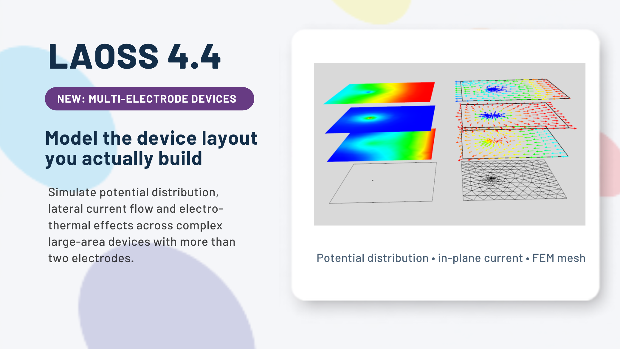
Figure 1. Simulation outputs for a three-electrode tandem device: potential distributions, in-plane currents and the finite-element mesh (shown in detail in Figure 2).
Moving from a small test device to a large-area cell, panel or module is rarely a simple matter of increasing its dimensions.
As the active area grows, finite electrode conductivity produces lateral voltage drops. Current distribution becomes non-uniform. Local defects can influence areas far beyond their physical dimensions. In solar cells, these effects can reduce fill factor and output power. In OLEDs and lighting panels, they can contribute to luminance non-uniformity, electrical losses and local heating.
These effects become more difficult to analyse when the device contains intermediate electrodes, segmented contacts or multiple electrically active junctions.
The central advance in Laoss 4.4
Laoss 4.4 removes the conventional two-electrode limitation and enables the electrical and electrothermal simulation of devices with more than a top and bottom electrode.
Why large-area devices behave differently
A local current-voltage curve describes charge transport through a small section of a device. It does not describe how current travels laterally through the electrodes before reaching the electrical contacts.
At larger device dimensions, electrode sheet resistance can lead to:
non-uniform potential distributions;
lateral current redistribution;
current crowding near contacts;
reduced fill factor and output power;
spatially varying OLED luminance;
localised ohmic heating;
sensitivity to contact position and electrode geometry; and
interaction between local defects and the surrounding device area.
Adding a highly conductive metal grid may reduce resistive losses, but it can also increase optical shadowing. Device design therefore involves a compromise between electrical conductivity, active area, optical performance and fabrication constraints.
Laoss connects the local electrical behaviour of a thin-film device with lateral transport across the complete device area. Its electrothermal model combines a two-dimensional finite-element representation of the electrodes with local one-dimensional current-voltage or current-voltage-temperature laws between adjacent electrodes.
Multi-electrode device simulation in Laoss 4.4
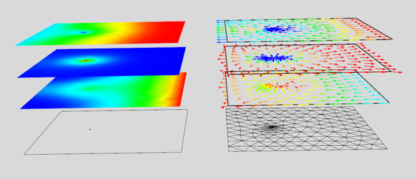
Figure 2. Example simulation of a tandem device with a local shunt. The results show potential distribution and in-plane current in the top, intermediate and bottom electrodes, together with the finite-element mesh.
Previous Laoss versions primarily supported conventional single-electrode or top-and-bottom-electrode configurations.
With Laoss 4.4, the model can contain more than two electrodes. Every pair of adjacent electrodes is connected through its own local coupling law.
A three-electrode device can therefore contain two separately defined electrical junctions:
1. the junction between the top and intermediate electrodes;
2. the junction between the intermediate and bottom electrodes.
Each junction can be described independently using an analytical expression, imported tabulated data or suitable device-simulation results.
This enables more realistic modelling of:
tandem and multi-junction solar cells;
conductive recombination or intermediate layers;
segmented electrodes;
pixelated devices;
complex module interconnections;
devices with multiple electrical terminals; and
localised shunts and inactive regions.
Electrode properties, electrical contacts and boundary conditions can be assigned to the relevant electrode. Sweeps can target a specific electrode or the cell between two neighbouring electrodes, making it possible to investigate how each conductive layer contributes to overall device behaviour.
See where performance is being lost
A global current-voltage curve shows that device performance has changed. It does not always show why.
Laoss provides spatially resolved simulation results that reveal the physical origin of large-area losses. Depending on the model configuration, users can evaluate:
potential distribution in individual electrodes;
lateral current flow;
current transferred between adjacent electrodes;
electrode ohmic losses;
temperature distribution;
heat flow;
total device current and power; and
solar-cell performance parameters.
This separates losses originating in the local thin-film stack from those introduced by the device layout.
Instead of only asking, “What is the final efficiency?”, researchers can investigate more useful design questions:
Where does the voltage drop occur?
Which electrode limits current collection?
How far does the influence of a local shunt extend?
Does an intermediate electrode redistribute current?
Which contact geometry provides the best balance between conductivity and active area?
Where are hot spots or thermal gradients likely to form?
Understanding the intermediate electrode in tandem solar cells
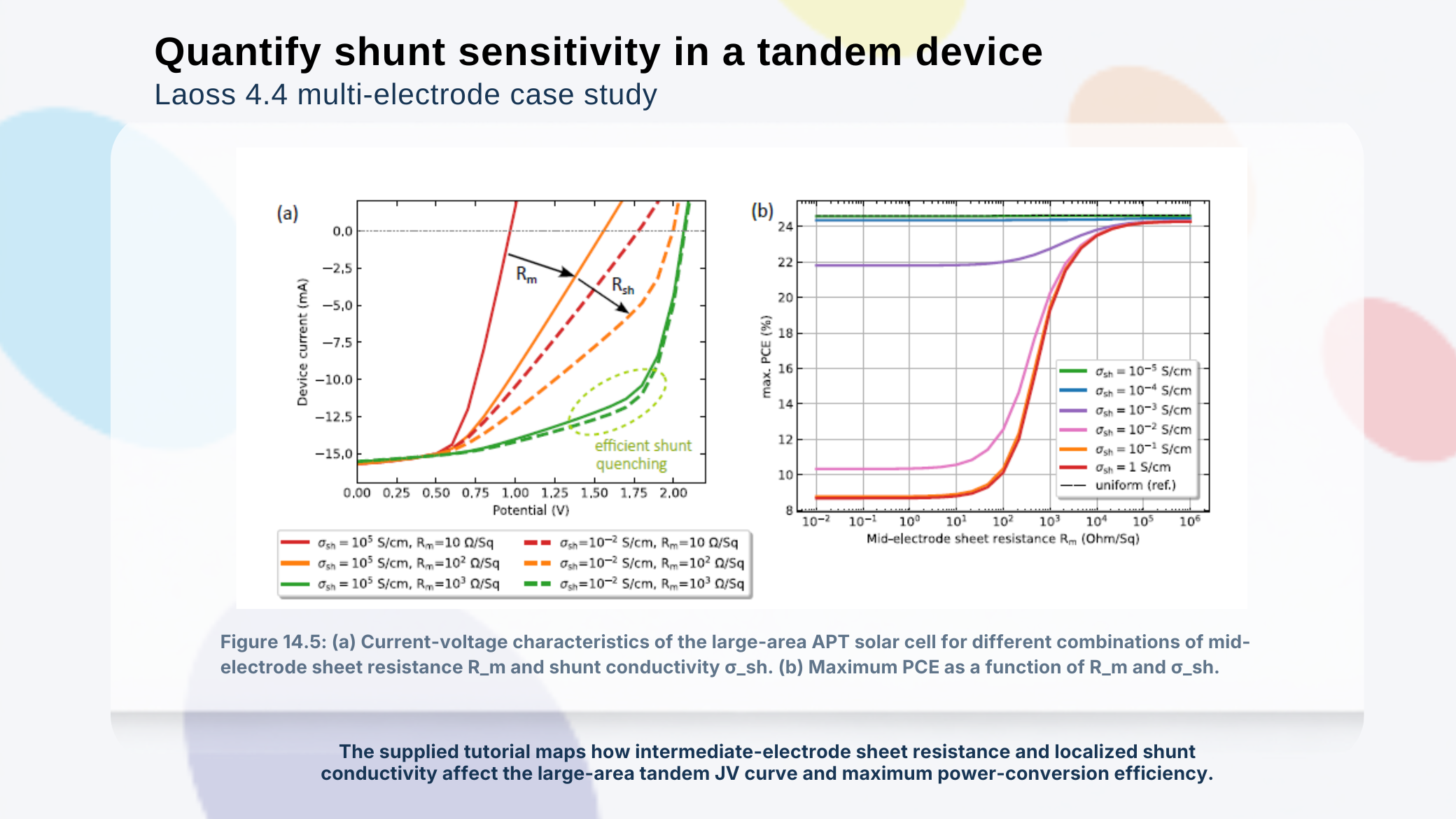
Figure 3. The Laoss 4.4 tutorial investigates how intermediate-electrode sheet resistance and a localised sub-cell shunt influence the current-voltage response and maximum power-conversion efficiency of the full tandem device.
The updated Laoss tutorial includes an all-perovskite tandem example containing a third, intermediate electrode.
The wide-bandgap and narrow-bandgap sub-cells are represented separately, while the lateral conductivity of the intermediate layer is included explicitly. A localised shunt is introduced into one of the sub-cells.
By varying the shunt conductivity and the sheet resistance of the intermediate electrode, the simulation shows how these parameters influence the JV curve and maximum power-conversion efficiency of the tandem device as a whole.
The numerical outcome is specific to the selected geometry and material parameters. However, the example demonstrates a more general capability: Laoss can connect a local defect or material property with its measurable effect at full device scale.
This relationship cannot be determined reliably from isolated small-area sub-cell JV curves alone.
From local measurements to the complete device
A typical Laoss electrothermal workflow consists of:
1. importing or defining the two-dimensional device geometry;
2. generating the finite-element mesh;
3. assigning the electrical properties of each electrode and subdomain;
4. defining the local coupling law between adjacent electrodes;
5. applying electrical contacts and boundary conditions;
6. sweeping parameters such as voltage, sheet resistance, geometry or defect conductivity; and
7. analysing spatial maps and global device characteristics.
Local coupling laws can be based on analytical equations, measured data or compatible simulation results.
This makes it possible to connect small-area characterisation and device-level modelling with the behaviour of the full solar cell, PV module, OLED panel or display structure.
Beyond electrical simulation
Laoss contains two principal simulation environments:
electrothermal finite-element simulation for large-area semiconductor devices; and
optical simulation using ray tracing.
The optical workflow can be used to study large-area optical structures, including layers, interfaces, non-planar surfaces, emission, reflection, transmission and far-field properties. Data generated by Fluxim tools such as Setfos, or measured using Paios or Phelos, can be imported into appropriate Laoss optical workflows.
Current scope
Optical and electrothermal simulations remain separate project types and are not directly coupled. For devices with more than two electrodes, electrothermal coupling is supported; AC simulations and the sequential coupled-electrode solver remain restricted to two-electrode configurations.
Design complex devices before fabrication
Laoss 4.4 makes it possible to evaluate how intermediate electrodes, multiple junctions, local defects, interconnections and contact layouts interact across a device.
This helps identify limitations before they are incorporated into a new prototype.
For teams developing tandem photovoltaics, large-area organic electronics, OLED panels or pixelated devices, Laoss 4.4 provides a more direct connection between the simulated device and the architecture that will actually be fabricated.
Model the layout you intend to build with Laoss 4.4.