Reverse-bias Stressing of Perovskite Solar Cells
Abstract
The limited long-term stability of perovskite solar cells (PSCs) remains a key barrier to commercialization, arising from a combination of intrinsic instabilities and extrinsic stressors (e.g., ion migration, air, heat, and illumination) that degrade performance during operation. At the module level, partial shading introduces an additional, highly relevant stress pathway—reverse-bias—adding a reliability challenge beyond single-cell degradation. Reverse-bias behaviour in PSCs is commonly discussed in the context of reverse-bias breakdown, characterized by an abrupt rise in reverse current density and often parameterized by the reverse breakdown voltage VBD with typical values reported in the −1 V to −5 V range and lower values achieved in recent reports. This breakdown is frequently attributed to band-to-band tunnelling at the electron transport layer with the effective field distribution modulated by ion-induced screening and thus dependent on ionic properties. Beyond breakdown-driven shunting, this work separates pre-breakdown degradation from shunting and shows that milder reverse-bias stressing induces progressive performance losses dominated by increased recombination without measurable changes in dominant mobile-ion signatures. Electroluminescence and photoluminescence imaging further reveal the reversible growth of "dark spots" at pristine "bright-spot" locations, indicating a local ionic origin that is nevertheless decoupled from irreversible global device degradation. These results underscore that low-current reverse-bias stress far below breakdown can still drive a distinct degradation pathway in PSCs, making it a critical commercialization concern separate from shunt-driven failure.
Introduction
Perovskite solar cells (PSCs) suffer from both intrinsic and extrinsic degradation mechanisms that undermine their long-term stability. Intrinsic factors as a result of the rich defect chemistry of halide perovskites, specifically under light [1], lead to processes such as ion migration from the perovskite layer to the charge transport layers causing irreversible efficiency loss [2]. Extrinsic stressors such as moisture, oxygen and ultraviolet (UV) light further degrade efficiency and lifespan. At the module level, additional stresses appear under realistic operating conditions, where partial shading or current mismatch between interconnected cells can drive the cells with lower photogeneration into reverse-bias, producing localized heating and thereby amplifying these intrinsic and extrinsic degradation pathways. [3]
Reverse-bias has long been a critical issue in established silicon PV module technology. It occurs when a shaded cell with reduced current output is connected in series with unshaded cells, forcing it into reverse-bias to maintain the same current through the string. This resulting power dissipation can raise the local temperature of the shaded cell tens of degrees above the rest of the module, leading to hot spots [4,5] that may cause performance loss, accelerated degradation, or even physical damage such as cell and glass cracking [6]. The problem is solved by adding a bypass diode in parallel as shown in Figure 1, which bypasses the current. As a result, the current running through the string including the shaded cell is small such that the dissipated power in the shaded cell is also small. This solves the hot spot heating problem in silicon modules.
However, as shown in Figure 1, the shaded cell is still strongly reverse-biased. When most of the current flows through the bypass diode and very little through the string containing the shaded and unshaded cells, the unshaded cells are at or close to VOC. The VOC of all these cells must be compensated for by a similar reverse-bias in the shaded cell, since the sum must equal the small parallel bypass diode voltage. This follows from Kirchhoff's voltage law, which dictates that the sum of voltages in a parallel connection must equal zero, so the voltage drop across the bypass diode must equal the sum of the voltage drops across the unshaded and shaded cells.
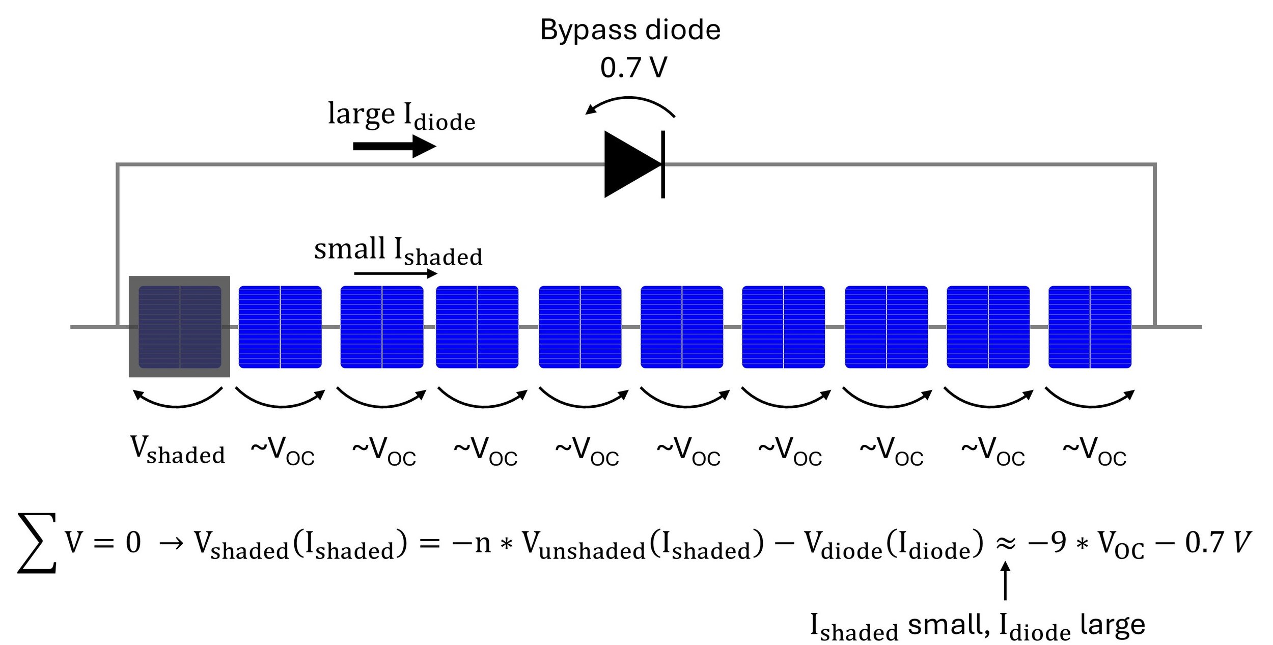
Figure 1. Reverse-bias across shaded cell in a parallel connection to a bypass diode under operating conditions. Adapted from [7]. Note that the voltage arrow indicates the direction of the voltage rise i.e. pointing from - to +.
One potential solution to high reverse-bias is placing a bypass diode across each individual cell, though this remains costly at scale. However, emerging PV technologies face scenarios where even this approach fails to fully prevent reverse-biasing. For instance, monolithic interconnected cells exhibit the same behaviour when one sub-cell is shaded as investigated in our previous simulation study of perovskite-silicon tandem solar cells [8]. Additionally, tandem cells - effectively two sub-cells in series - suffer current mismatch between top and bottom junctions, driving one into reverse-bias during operation as illustrated in Figure 2 and detailed in previous analysis [9,10]. However, in this case, the maximum reverse-bias on the perovskite sub-cell is limited to approximately one open-circuit voltage in tandem.
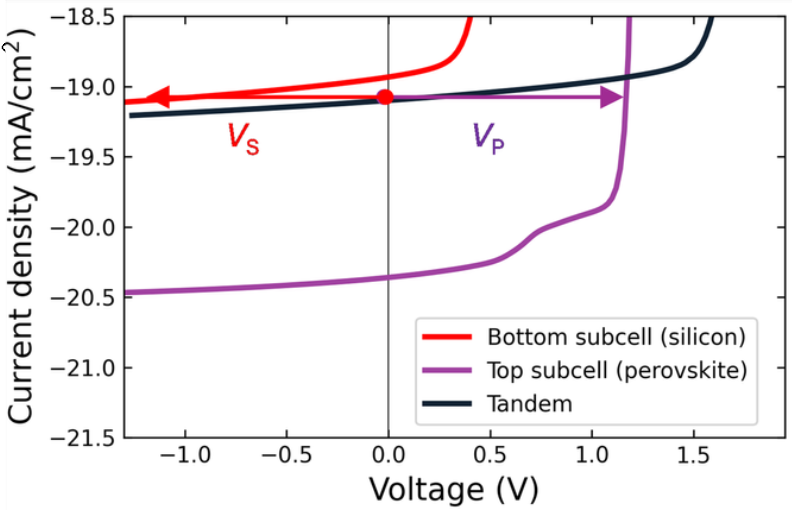
Figure 2. Close-up of a current density–voltage curve of a tandem cell with non-ideal current matching of the two sub-cells. The working points of the tandem and the sub-cells are indicated for operation of the tandem at 0 V. Detailed description can be found in [9].
Reverse-bias breakdown in perovskite solar cells is frequently characterized by an abrupt increase in reverse current density. The reverse breakdown voltage (VBD) has been defined as the point where current density reaches -1 mA/cm² [11,12]. Typical VBD values range from -1 V to -5 V [13], though recent advances have achieved -8 V and lower [14]. This breakdown originates from band-to-band tunnelling at the electron transport layer (ETL) [13–15], also termed Zener breakdown [8,16]. Consequently, the experimental reverse-bias breakdown of p-i-n structured perovskite solar cells varies significantly depending on the HTL used. [14,17] The strong electric fields under reverse-bias are further modulated by ion-induced field screening, making the breakdown voltage depend on ion density—as explored in prior work [8]. Higher ion densities amplify electric fields near contacts and thus tunnelling currents, as depicted in Figure 3b. The tunneling model leading to reverse-bias breakdown is described in [6] while details about the solar cell stack and the employed material parameters for this simulation can be found in [18].
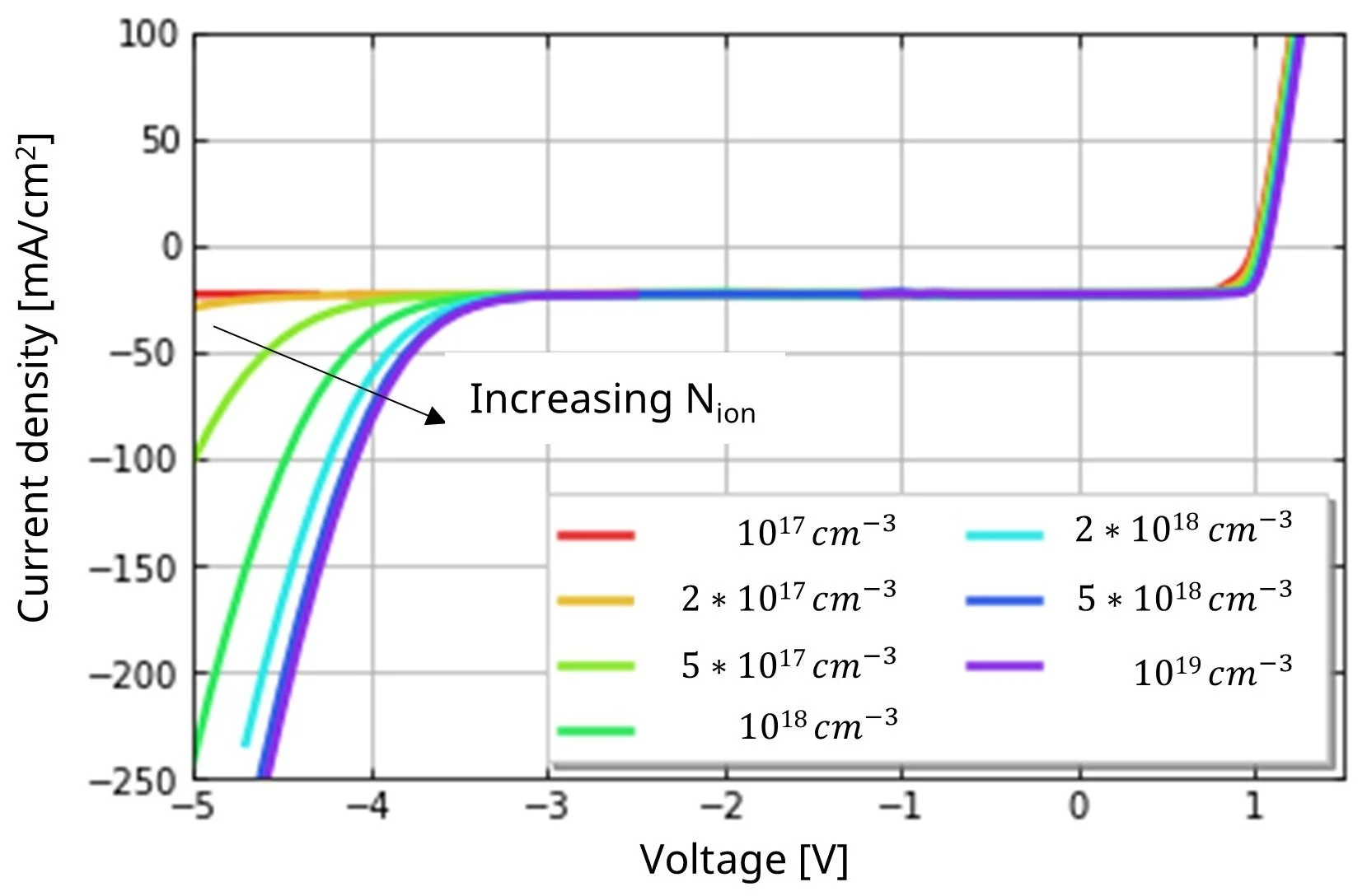
Figure 3. Simulated breakdown voltage dependence on the ion density. The model includes band-to-band tunnelling which is available in Setfos 6.0.
Reaching the breakdown voltage VBD rapidly induces shunt formation. [15] Consequently, most reverse-bias research focuses on increasing VBD. Tunneling at the ETL oxidizes halides (in either ETL or HTL), with the resulting halogens acting as recombination centers. The formed iodine radicals may either oxidize further via holes or react with electrodes to produce metal cations.[15,19,20] The incorporation of mobile metal ions into the perovskite layer can create conductive shunt paths. [15] These findings suggest that reverse-bias degradation occurs through the creation of recombination centres, which takes place prior to breakdown and, in principle, independently of shunting. However, detailed studies of sub-VBD initial degradation remain scarce, and experimental separation of early degradation from shunting requires further investigation—which we address in this work.
Methods
This study was conducted on p-i-n perovskite solar cells (PSCs) from the PVlab research institute at the École Polytechnique Fédérale de Lausanne (EPFL) [21]. These PSCs contain a perovskite active layer with a bandgap of 1.48 eV. This layer is sandwiched between a self-assembled monolayer (SAM) of hole transport material and a layer of fullerene C60 for electron transport. In order to reduce VBD to a level at which studying the initial degradation process becomes feasible, an SnO₂ ALD layer was deposited on top of the C60 layer. [15]
To characterise the effects of reverse-bias on PSCs, we employ a novel combination of experimental techniques. Previous research has primarily focused on current-voltage (I-V) analysis and, to a lesser extent, infrared thermography [11,22,23] or electroluminescence/photoluminescence (EL/PL) imaging [24]. In contrast, our study integrates impedance spectroscopy (IS) and transient electrical measurements with Paios to directly monitor ionic charge transport (see Figure 4). This is coupled with EL/PL mapping using our multi-spectral imaging tool, “Vitios”, which is able to spatially and temporally resolve degradation patterns across the device. Vitios is currently being developed as part of the DICE Eurostars/Horizon Europe project and will soon be available.
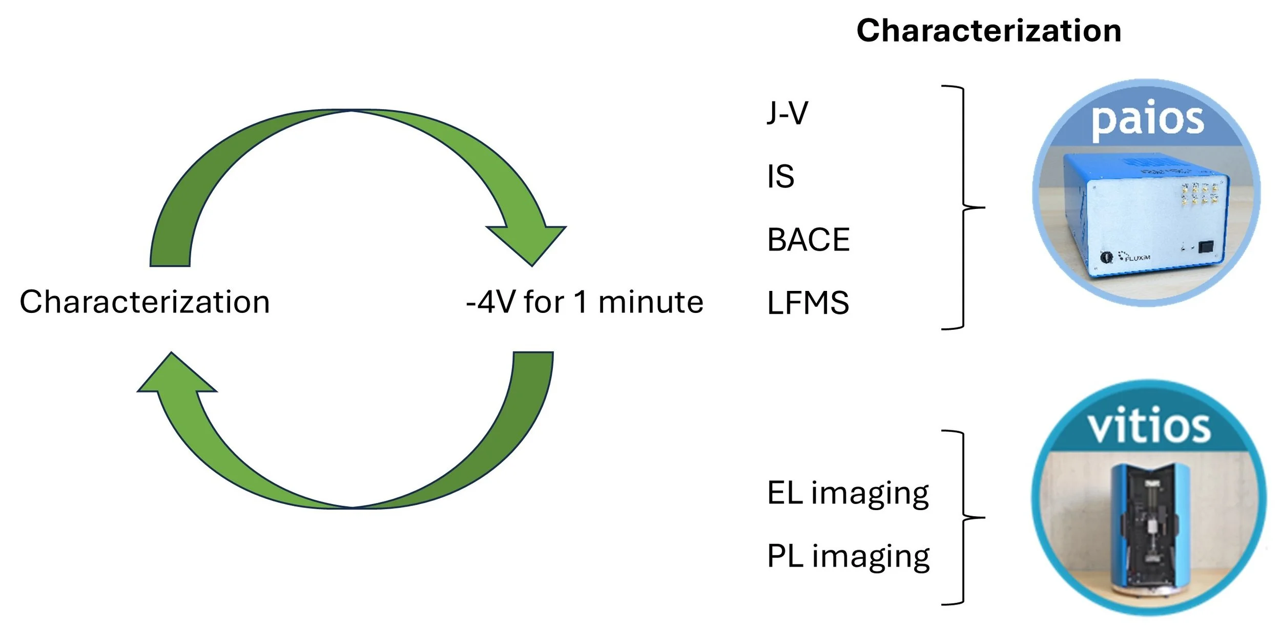
Figure 4. Measurement protocol for reverse-bias stressing. Note that two equivalent device pixels on the same cell are measured with the two systems.
Explore electrical characterization with Paios
Paios supports advanced electrical characterization for perovskite solar cells, including J-V, impedance spectroscopy, transient measurements, BACE and LFMS. If you would like to investigate ionic effects, recombination losses and device stability in more detail, explore Paios or get in touch with our team.

Results and discussion
The characterisation routine in Figure 4 has been used to investigate the effect of consecutive exposure to reverse-bias on the electrical response and luminescence properties of the samples. First, the intermittent measurements were tested using open- or short-circuit conditions instead of reverse-bias, which only had a negligible influence on the cell performance. In other words, the characterisation itself does not notably affect the device's performance.
Exploration of the breakdown voltage
To determine an appropriate reverse-bias voltage prior to breakdown, the following steps are taken:
Exploration of the breakdown voltage. Figure 5a shows the current density measurements obtained for a small number of reverse bias voltages, in order to minimise degradation.
Application of stress for a set time at a constant negative bias (V < VBD).
Decrease/increase V and repeat the stress process until a bias is found without shunting the device within the defined time and a noticeable decrease in PV performance occurs.
A set of devices was subjected to reverse-bias stressing at -5 V (Figure 5b), resulting in a very rapid degradation of device performance. Full shunting of the device occurred within three minutes of stressing. Although -5 V is above VBD, it exceeds the range for which reverse-bias stressing is useful in analysing degradation dynamics, as catastrophic failure mechanisms linked to reverse-bias breakdown occur rapidly. A reverse-bias of -4 V (Figure 5c) strikes a balance between accelerated degradation and device survival. Over six cycles, a moderate decrease in VOC and FF was observed, resulting in a power conversion efficiency (PCE) loss from 18.5% to 16.8%. Although degradation is evident, the devices do not show shunting. This is indicated by minor changes around 0 V in the dark JV curves (Figure 5d). Note that the increase in dark injection current correlates with the decrease in VOC. Table 1 summarises performance changes for reverse-biases of -3 V, -4 V and -5 V.
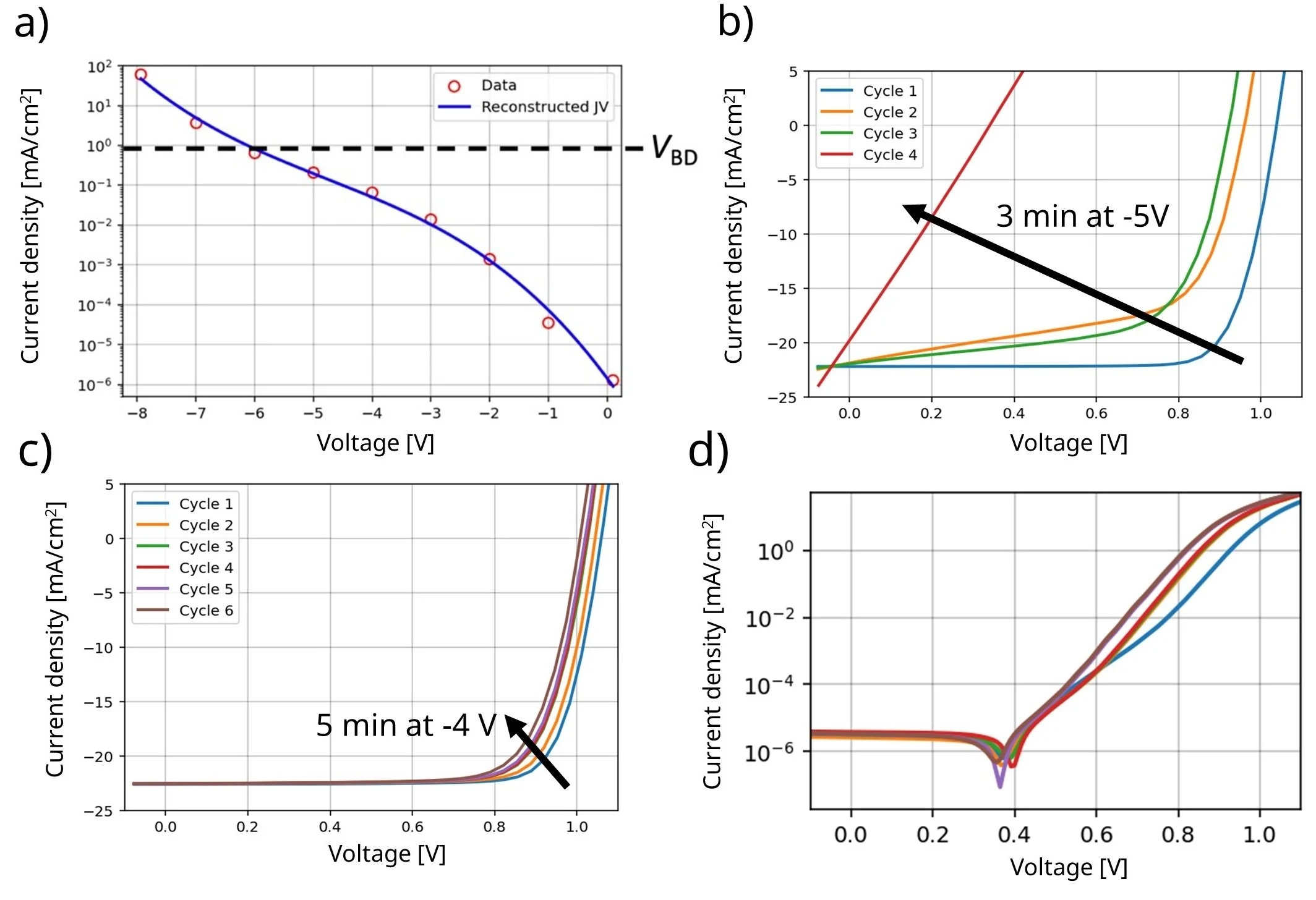
Figure 5. a) Reverse-bias current densities were measured at individual voltages, with the breakdown voltage (VBD) indicated. JV curves measured between reverse-bias stressing b) at -5 V and c) at -4 V. d) Dark JV curves measured between reverse-bias stressing at -4 V.
Table 1. Device performance before and after reverse-bias stressing procedure at various voltages. The initial performance of all devices is very similar. The PCE was measured using a white LED illumination equivalent to 1 sun.
| VOC (V) | FF (-) | JSC (mA cm-2) | PCE (%) | ||
|---|---|---|---|---|---|
| -3 V | t = 0 min Cycle 1 | 1.04 | 0.78 | 22.9 | 18.4 |
| t = 5 min Cycle 6 | 1.02 | 0.77 | 22.8 | 17.9 | |
| -4 V | t = 0 min Cycle 6 | 1.04 | 0.79 | 22.7 | 18.5 |
| t = 5 min Cycle 6 | 0.97 | 0.76 | 22.6 | 16.8 | |
| -5 V | t = 0 min Cycle 6 | 1.04 | 0.79 | 22.2 | 18.2 |
| t = 3 min Cycle 4 | 0.34 | 0.26 | 19.8 | 1.7 |
Ion-sensitive measurements
To elucidate the origins of reverse-bias-induced changes, we distinguish ionic- from recombination-sensitive measurements. These include bias-assisted charge extraction (BACE), in which the device is held near VOC to reach an ionic steady state before switching to 0 V to trigger ionic drift currents - a method that has linked rising ion densities to operational degradation [25]. Figure 6a displays BACE current transients measured between the -4 V reverse-bias stress periods, revealing minimal changes. Since the initial current density scales with mobile ion conductivity (i.e., ion density times mobility) [26], this implies stable ionic properties. Typically, mobile ion charge density is obtained by integrating the BACE transient; however, with sufficient high bulk ion density the integrated charge reflects the ion density necessary to screen the electric field rather than total bulk density. [26,27] In this case an appropriate model of the depletion region at the interface is necessary to calculate a bulk ion density [28]. The second measurement is low-frequency Mott-Schottky (LFMS) analysis. It has been shown that LFMS provides more accurate quantification of mobile ion bulk densities when the mobile ion density is higher than the limit to screen the electric field. By making use of the depletion approximation, a linear approximation of the inverse squared capacitance as a function of bias voltage directly yields the mobile ion density. [27]
Figure 6b shows an overview of the calculated mobile ion densities obtained from both BACE and LFMS between reverse-bias stressing at -4 V. The mobile ion density as obtained from BACE is approximately one order of magnitude lower than the value from LFMS as reported previously for high ion densities [27]. However, it is more relevant that neither ion density exhibits any significant change during reverse-bias stressing. In our drift-diffusion model of the cells [18], the LFMS analysis of the low-frequency capacitance-voltage simulation results in a similar lower ion density of 1017 to 1018 cm-3, while the input bulk ion density is 1019 cm-3. This means that the LFMS analysis underestimates the bulk ion density in our model as well, since it is limited by contact capacitance rather than ionic capacitance. In our case, this is the C60 capacitance [18]. Nevertheless, the model also shows that altering the bulk ion density results in a change in the extracted ion density from the LFMS analysis, indicating its sensitivity to changes in the bulk ion density.
The conclusions from these measurements must be stated cautiously. Unaltered BACE transient initial current densities indicate stable ion conductivity, while unchanged integrated charge densities imply no variation in bulk electric field screening parameters (ionic capacitance and ion density required for electric field screening). Consistent LFMS densities suggest no change in bulk ion density. Importantly, these findings relate only to the dominant bulk ion species; slower-timescale ion-related electrochemical processes linked to reverse-bias degradation may remain undetected by these methods.
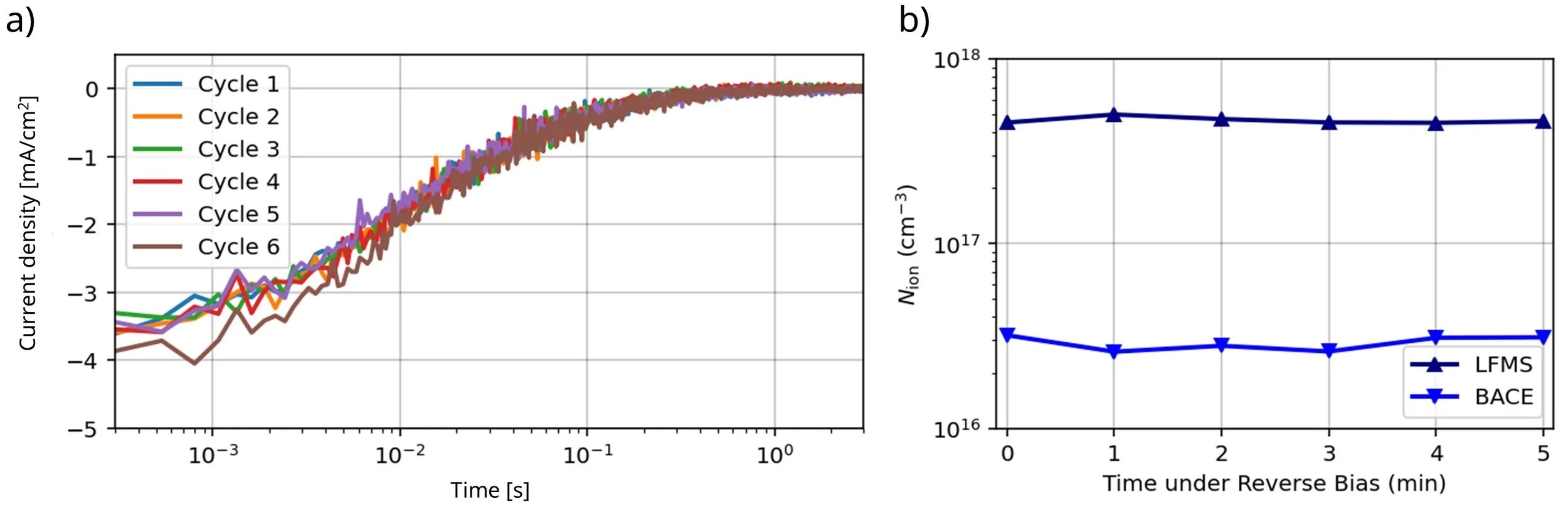
Figure 6. a) BACE current transients and b) calculated mobile ion densities from BACE and LFMS between reverse-bias stressing at -4 V for 1 min per cycle.
Capacitance-frequency analysis
Similar conclusions emerge from full capacitance–frequency spectra recorded between reverse-bias stressing at -4 V (Figure 7). As detailed in our recent blog post[18], low frequency capacitance level in the dark is sensitive to the bulk ion density, as also simulated in Figure 7b. The ion mobility (Figure 7c) shifts the ionic redistribution time constant, i.e. the transition frequency between low- and high-frequency capacitance levels, without altering them. These results must again be interpreted cautiously regarding slower ion-related electrochemistry. If such processes drive the observed degradation — as suggested by literature [11,15,19] — then formed recombination centres related to the oxidation of halides appear sufficiently potent to impact performance, even though the associated ion density remain far below the bulk levels governing the low-frequency capacitance signal.
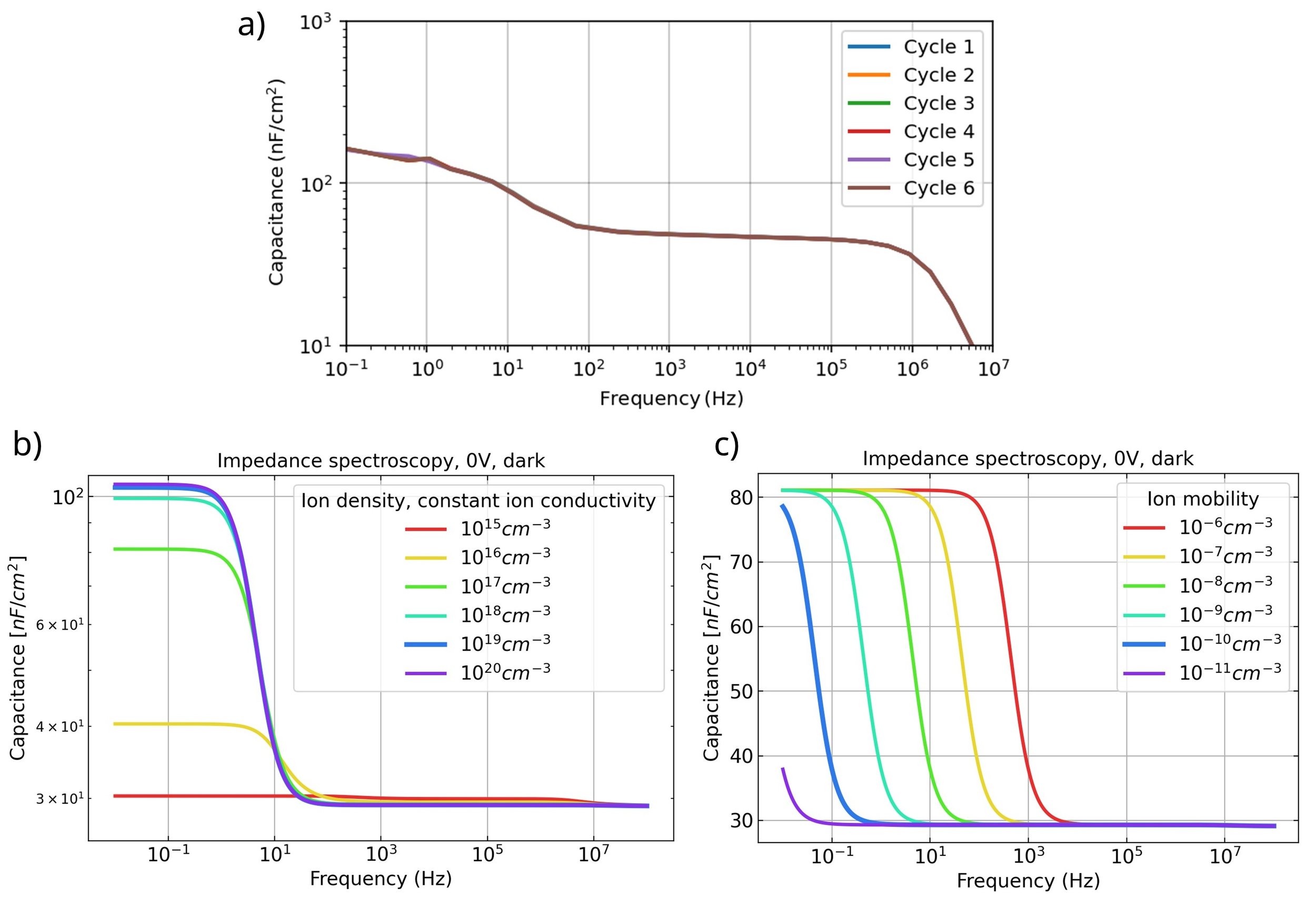
Figure 7. a) Capacitance–frequency spectra between reverse-bias stressing b) The bulk ion density influences the low frequency capacitance level. c) Varying the mobility of ions influences the time constant of the ionic redistribution, i.e. the transition frequency. Note that the time constant is inversely proportional to the ion conductivity, i.e. the ion density and mobility product. Therefore, the ion density also changes the time constant and transition frequency, unless the product and therefore the ion conductivity is kept constant while changing the ion density as done in b).
EL and PL imaging
To better understand effects of reverse-bias on recombination, EL imaging was performed at 1 V (≈VOC). Figure 8 shows EL maps of a PSC measured at 1 V for 60 s between stressing at -4 V: The overall EL intensity diminishes markedly, while the pristine device exhibits initially bright spots that progressively darken with continued stress cycles. This is quantified in Figure 8b, where relative EL intensity across the device drops ~40% after 5 min of -4 V stressing — even as current density at 1 V rises from ~4 to ~14 mA/cm². Without altered recombination pathways, higher injection current should boost EL intensity, contrary to observations, thus indicating substantially increased non-radiative recombination. Photoluminescence (PL) measurements at open circuit (Figure 9) confirm elevated overall non-radiative losses, with the stressed central pixel showing reduced PL intensity relative to pristine outer pixels under uniform UV excitation. This implies lower photoluminescence quantum yield (PLQY), and non-radiative losses scale with ln(PLQY). [29]
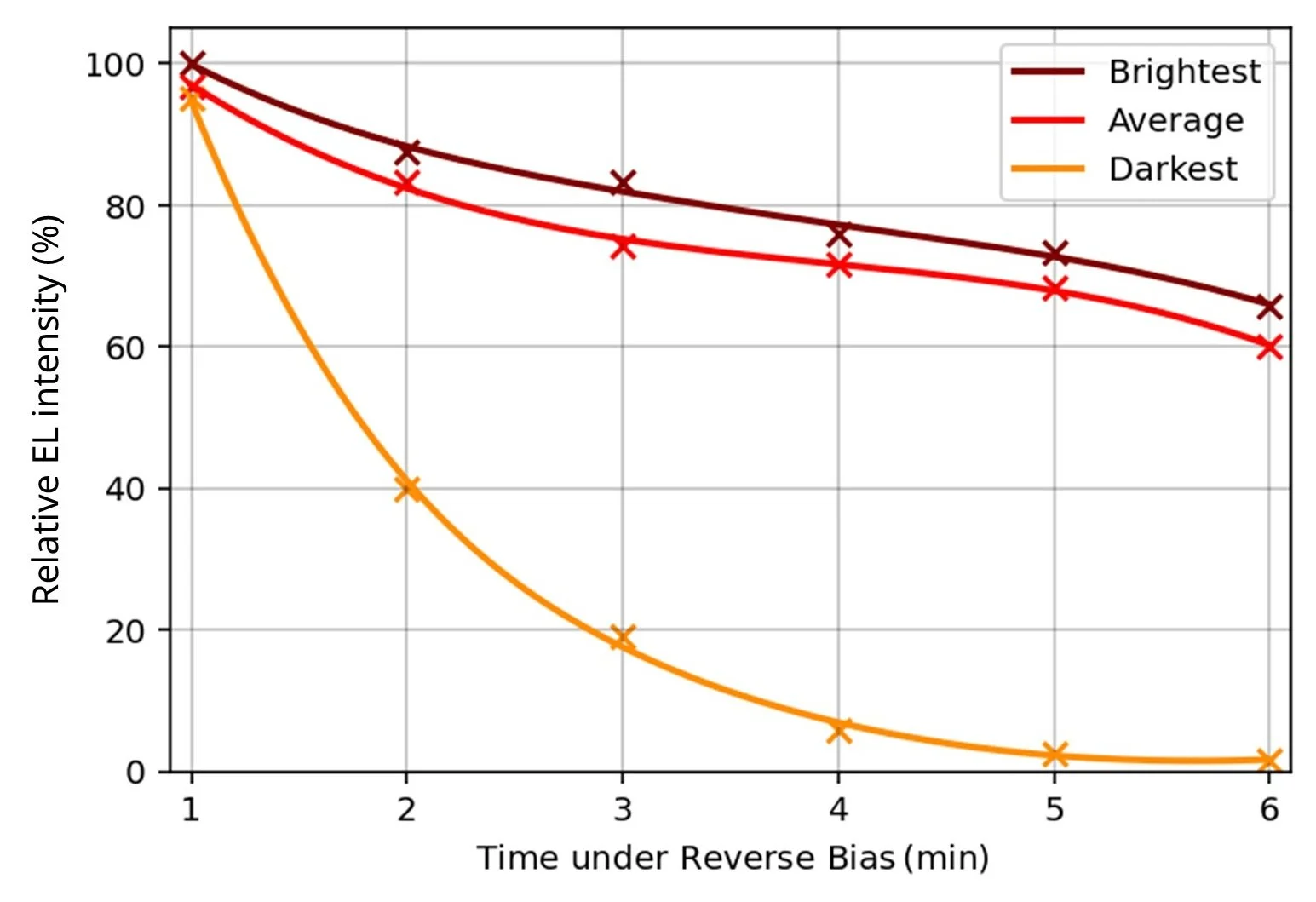
Figure 8. a) Series of EL images at 1.15 V taken in between 30s reverse-bias stressing cycles at -4 V b) Relative EL intensities of a growing dark spot and the remaining bright area (different pixel than a).
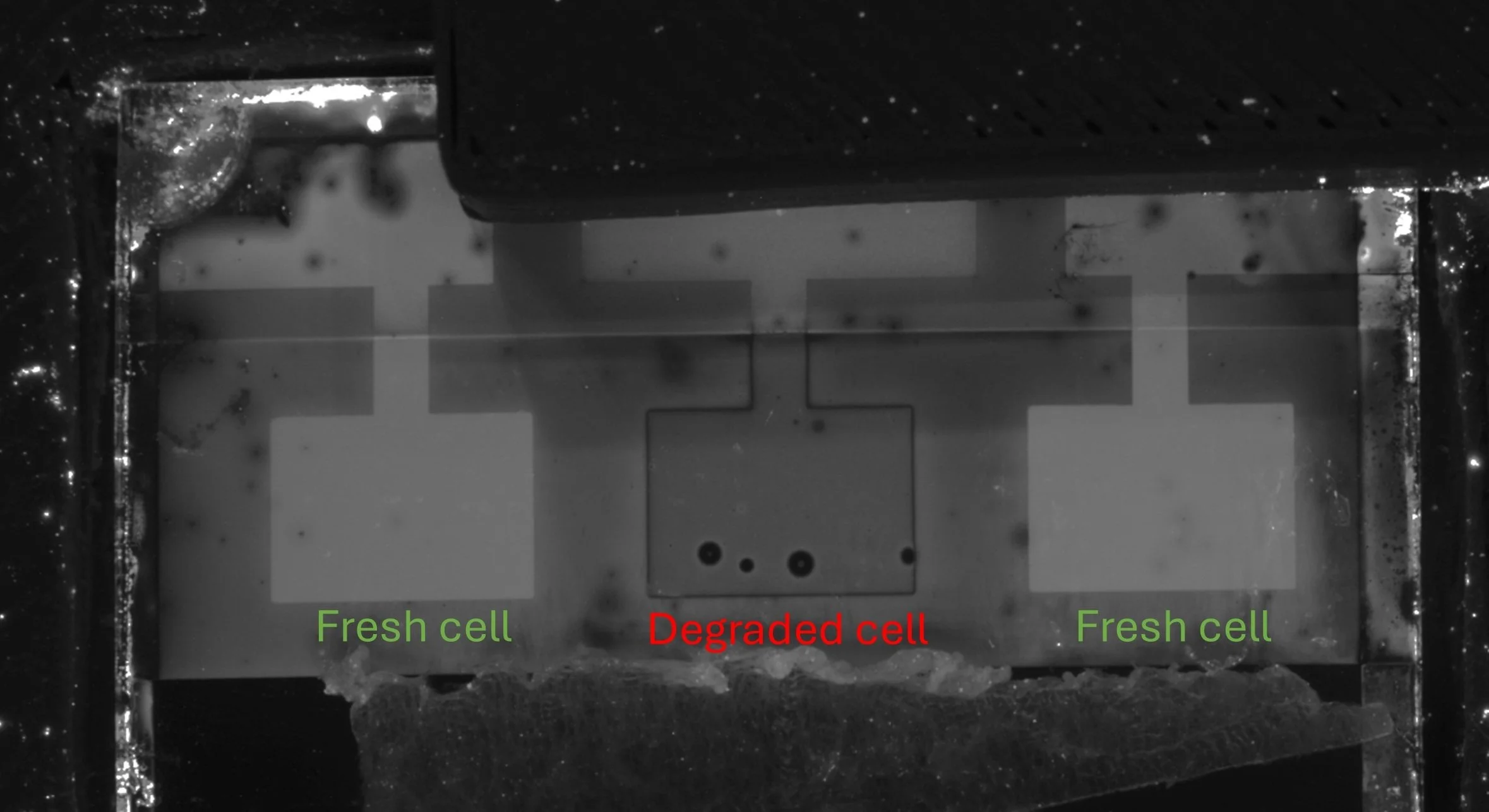
Figure 9. PL image of three pixels at open circuit, where the centre pixel experienced a reverse-bias stressing at -4 V for 5 minutes.
Dark spot coverage and device performance
To understand the effect of dark spots on device degradation, two devices with different levels of spot coverage were tested and compared (see Figure 10). It can be seen here that the two devices exhibit almost equivalent performance, with PCEs of 18.9% and 18.8% respectively, despite the significant difference in the number of bright spots. Additionally, after reverse-bias stressing, the performance of both devices remains equivalent, but the dark spot coverage relative to the total device area varies substantially. This implies that there is no correlation between the area of the affected spots and device performance as measured in JV sweeps. We can conclude that the spots do not affect the unaffected regions, for example through shunting behaviour. However, we cannot rule out reduced efficiency within the area covered by the spots (e.g. a reduced short circuit current or Voc within the spot area, which would have a minor impact on overall performance).
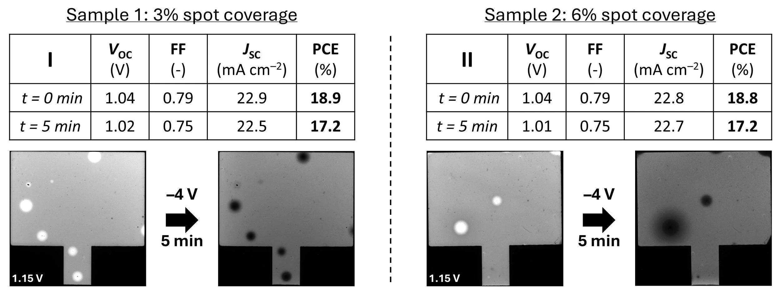
Figure 10. Comparison of two devices between reverse-bias stressing at -4 V, where one device has low dark spot coverage and the other device has higher dark spot coverage. In both cases, the initial device performance is similar, as well as the device performance after reverse-bias stressing.
Reversibility after storage
To assess whether the observed PSC degradation under reverse-bias relates to reversible ionic effects, the devices were stored for 4 weeks in dry air and light vacuum before repeating the measurement protocol. Figure 11a reveals no performance recovery post-storage: illuminated JV curves show persistent VOC and FF losses, suggesting irreversible overall degradation. The same applies to fully shunted devices stressed near or above breakdown, which remained shunted.
In contrast, EL maps in Figure 11b demonstrate reversible spot dynamics. After 4-week storage, dark spots revert to bright, and subsequent stressing again produces dark spots. This reveals bright-to-dark spot conversion as reversible, unlike global degradation, and may relate to local ion density fluctuations causing hot-spot heating as explored previously [8] or to the transient bright spots we modelled in printed mesoporous TiO2–carbon PSCs via coupled 1D drift-diffusion and 2D+1D FEM simulations of locally enhanced ion densities. [30]
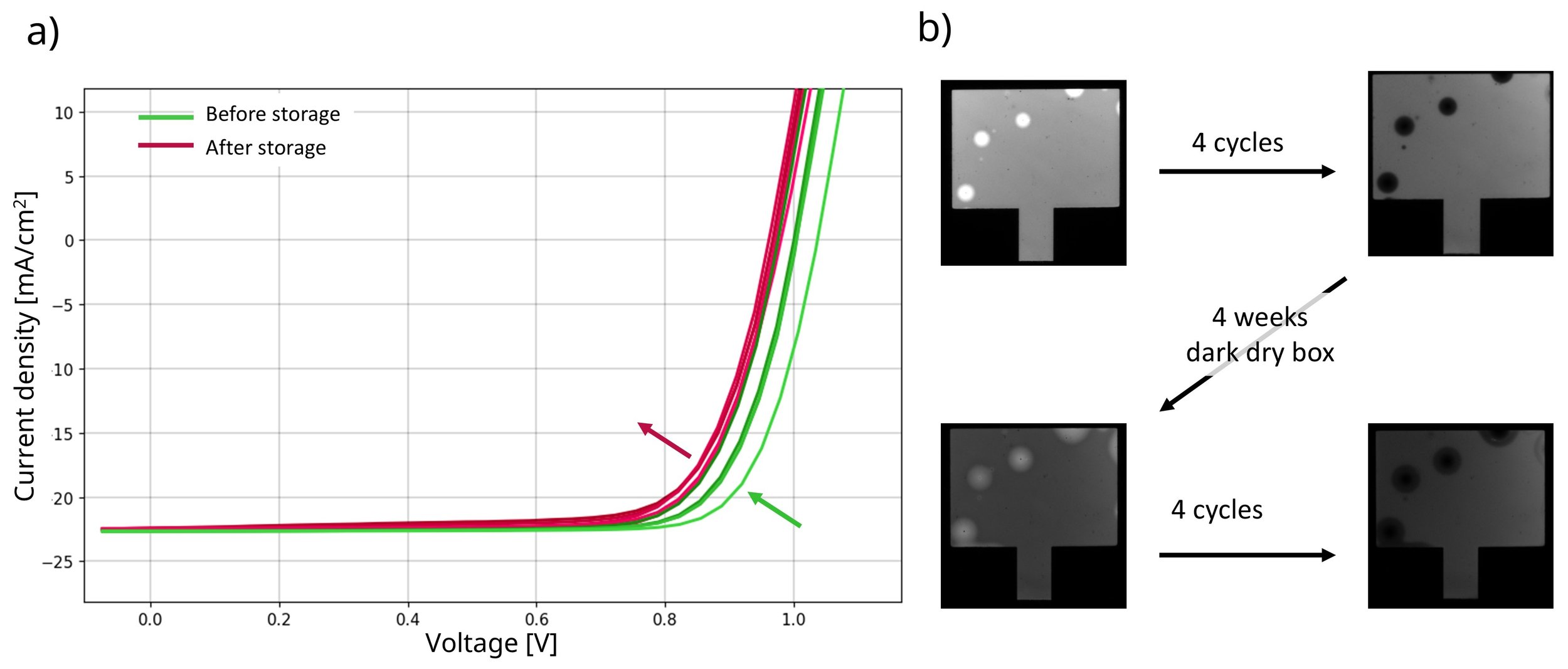
Figure 11. a) J-V curves under 1-sun equivalent illumination and b) EL maps at 1.15V (different pixel than in a). The samples were reverse-biases at -4 V for four 1-minute cycles (green curves). After the device was stored in dry air and light vacuum for 4 weeks and then the reverse-bias protocol was repeated (red curves).
Conclusion and outlook
We distinguish reverse-bias breakdown (shunting) from pre-breakdown degradation. Breakdown occurs abruptly for applied voltages close to or below VBD, causing instant device shorting. In contrast, for applied biases that do not reach the breakdown voltage, recombination increases progressively, manifesting as VOC and FF losses without shunting. Notably, measurements sensitive to the dominant mobile ion species — dark 0 V capacitance spectra, BACE, and LFMS—show no changes in either regime.
A striking feature is the growth of fully circular dark spots emerging precisely at bright spot locations in pristine EL maps. These are not shunts, nor do they correlate with overall device degradation. Their reversibility strongly implicates an ionic process rather than permanent structural damage.
The findings highlight that reverse-bias degradation at low current densities — well below breakdown — poses a critical challenge for perovskite solar cell (PSC) commercialisation, which is distinct from shunt formation. Although our investigated system exhibits negligible degradation under mild reverse-bias (from −0.5 to −1 V) over short timescales of minutes, the long-term effects of this reverse-bias range happening in mismatched tandems or even in per-cell bypassed modules remain unclear, particularly under prolonged shading spanning days or weeks.
Acknowledgements
We thank Ralph van den Heuvel from Eindhoven University of Technology for his work during his internship. He performed all the measurements featured in this blog post and provided an extensive report as a basis for it. We thank Mostafa Othman for fabricating the devices. This work has been benefited from financial support of the DICE Eurostars/Horizon Europe project. Eurostars is part of the European Partnership on Innovative SMEs. The partnership is co-funded by the European Union through Horizon Europe. This study was supported by the Swiss National Science Foundation via SINERGIA project “RADICALS”, grant no. CRSII5_216647.


References
1. Moia D, Maier J. Defect chemistry of mixed ionic–electronic conductors under light: halide perovskites as a master example. Mater Horiz. 2026;10.1039.D5MH01231G. doi:10.1039/D5MH01231G
2. Shen Z, Han Q, Luo X, Shen Y, Wang Y, Yuan Y, et al. Efficient and stable perovskite solar cells with regulated depletion region. Nat Photonics. 2024 May;18(5):450–7. doi:10.1038/s41566-024-01383-5
3. Baumann S, Eperon GE, Virtuani A, Jeangros Q, Kern DB, Barrit D, et al. Stability and reliability of perovskite containing solar cells and modules: degradation mechanisms and mitigation strategies. Energy Environ Sci. 2024;17(20):7566–99. doi:10.1039/D4EE01898B
4. Bothe K, Ramspeck K, Hinken D, Schinke C, Schmidt J, Herlufsen S, et al. Luminescence emission from forward- and reverse-biased multicrystalline silicon solar cells. J Appl Phys. 2009 Nov 15;106(10):104510. doi:10.1063/1.3256199
5. Breitenstein O, Bauer J, Bothe K, Kwapil W, Lausch D, Rau U, et al. Understanding junction breakdown in multicrystalline solar cells. J Appl Phys. 2011 Apr 1;109(7):071101. doi:10.1063/1.3562200
6. Dhimish M, Lazaridis PI. An empirical investigation on the correlation between solar cell cracks and hotspots. Sci Rep. 2021 Dec 14;11(1):23961. doi:10.1038/s41598-021-03498-z
7. Honsberg CB, Bowden SG. Photovoltaics Education Website [Internet]. [cited 2025 Dec 1]. Available from: https://www.pveducation.org/pvcdrom/modules-and-arrays/bypass-diodes
8. Aeberhard U, Natsch N, Schneider A, Zeder SJ, Carrillo‐Nuñez H, Blülle B, et al. Multi‐Scale Simulation of Reverse‐Bias Breakdown in All‐Perovskite Tandem Photovoltaic Modules under Partial Shading Conditions. Sol RRL. 2024 Nov;8(21):2400492. doi:10.1002/solr.202400492
9. Moia D. Investigating Current Matching and Hysteresis in Perovskite-Silicon Tandem Solar Cells with Drift-Diffusion Simulations [Internet]. Available from: https://www.fluxim.com/research-blogs/current-matching-perovskite-silicon-tandem-solar-cells
10. Messmer C, Chojniak D, Bett AJ, Reichmuth SK, Hohl‐Ebinger J, Bivour M, et al. Toward more reliable measurement procedures of perovskite‐silicon tandem solar cells: The role of transient device effects and measurement conditions. Prog Photovolt Res Appl. 2025 Jan;33(1):126–42. doi:10.1002/pip.3782
11. Bowring AR, Bertoluzzi L, O’Regan BC, McGehee MD. Reverse Bias Behavior of Halide Perovskite Solar Cells. Adv Energy Mater. 2018 Mar;8(8):1702365. doi:10.1002/aenm.201702365
12. Henzel J, Bakker K, Najafi M, Zardetto V, Veenstra S, Isabella O, et al. Impact of the Current on Reverse Bias Degradation of Perovskite Solar Cells. ACS Appl Energy Mater. 2023 Nov 27;6(22):11429–32. doi:10.1021/acsaem.3c02273
13. Wang C, Huang L, Zhou Y, Guo Y, Liang K, Wang T, et al. Perovskite Solar Cells in the Shadow: Understanding the Mechanism of Reverse‐Bias Behavior toward Suppressed Reverse‐Bias Breakdown and Reverse‐Bias Induced Degradation. Adv Energy Mater. 2023 Mar;13(9):2203596. doi:10.1002/aenm.202203596
14. Jiang F, Shi Y, Rana TR, Morales D, Gould IE, McCarthy DP, et al. Improved reverse bias stability in p–i–n perovskite solar cells with optimized hole transport materials and less reactive electrodes. Nat Energy. 2024 Aug 7;9(10):1275–84. doi:10.1038/s41560-024-01600-z
15. Li N, Shi Z, Fei C, Jiao H, Li M, Gu H, et al. Barrier reinforcement for enhanced perovskite solar cell stability under reverse bias. Nat Energy. 2024 Jul 1;9(10):1264–74. doi:10.1038/s41560-024-01579-7
16. Kane EO. Zener tunneling in semiconductors. J Phys Chem Solids. 1960 Jan;12(2):181–8. doi:10.1016/0022-3697(60)90035-4
17. Morales DA, Sindt C, Fremouw K, Mao K, Poma M, Stewart T, et al. Nickel-oxide hole-transport layers prevent abrupt reverse-bias breakdown and permanent shorting of perovskite solar cells caused by pinhole defects. EES Sol. 2026;10.1039.D5EL00206K. doi:10.1039/D5EL00206K
18. Moia D. Setfos modeling of halide perovskite solar cells with focus on their mixed ionic-electronic conducting properties: a step-by-step tutorial [Internet]. Available from: https://www.fluxim.com/research-blogs/stutorial-setfos-pscs-ionic-properties
19. Bertoluzzi L, Patel JB, Bush KA, Boyd CC, Kerner RA, O’Regan BC, et al. Incorporating Electrochemical Halide Oxidation into Drift-Diffusion Models to Explain Performance Losses in Perovskite Solar Cells under Prolonged Reverse Bias. Adv Energy Mater. 2021 Mar 1;11(10):1–9. doi:10.1002/aenm.202002614
20. Ni Z, Jiao H, Fei C, Gu H, Xu S, Yu Z, et al. Evolution of defects during the degradation of metal halide perovskite solar cells under reverse bias and illumination. Nat Energy. 2022 Jan;7(1):65–73. doi:10.1038/s41560-021-00949-9
21. Othman M, Jeangros Q, Jacobs DA, Futscher MH, Zeiske S, Armin A, et al. Alleviating nanostructural phase impurities enhances the optoelectronic properties, device performance and stability of cesium-formamidinium metal–halide perovskites. Energy Environ Sci. 2024;17(11):3832–47. doi:10.1039/D4EE00901K
22. Bogachuk D, Saddedine K, Martineau D, Narbey S, Verma A, Gebhardt P, et al. Perovskite Photovoltaic Devices with Carbon‐Based Electrodes Withstanding Reverse‐Bias Voltages up to –9 V and Surpassing IEC 61215:2016 International Standard. Sol RRL. 2022 Mar;6(3):2100527. doi:10.1002/solr.202100527
23. Razera RAZ, Jacobs DA, Fu F, Fiala P, Dussouillez M, Sahli F, et al. Instability of p–i–n perovskite solar cells under reverse bias. J Mater Chem A. 2020;8(1):242–50. doi:10.1039/C9TA12032G
24. Aninat R, Bakker K, Henzel J, Zardetto V, Dogan I, Gevaerts V, et al. Mapping the Partial Shading Degradation in a Monolithically Integrated Perovskite Module. Prog Photovolt Res Appl. 2025 Jan 30;pip.3881. doi:10.1002/pip.3881
25. Thiesbrummel J, Shah S, Gutierrez-Partida E, Zu F, Peña-Camargo F, Zeiske S, et al. Ion-induced field screening as a dominant factor in perovskite solar cell operational stability. Nat Energy. 2024 Mar 28;9(8):664–76. doi:10.1038/s41560-024-01487-w
26. Diethelm M, Lukas T, Smith J, Dasgupta A, Caprioglio P, Futscher M, et al. Probing ionic conductivity and electric field screening in perovskite solar cells: a novel exploration through ion drift currents. Energy Environ Sci. 2025;18(3):1385–97. doi:10.1039/D4EE02494J
27. Diekmann J, Peña-Camargo F, Tokmoldin N, Thiesbrummel J, Warby J, Gutierrez-Partida E, et al. Determination of Mobile Ion Densities in Halide Perovskites via Low-Frequency Capacitance and Charge Extraction Techniques. J Phys Chem Lett. 2023 May 11;14(18):4200–10. doi:10.1021/acs.jpclett.3c00530
28. Bertoluzzi L, Boyd CC, Rolston N, Xu J, Prasanna R, O’Regan BC, et al. Mobile Ion Concentration Measurement and Open-Access Band Diagram Simulation Platform for Halide Perovskite Solar Cells. Joule. 2020 Jan;4(1):109–27. doi:10.1016/j.joule.2019.10.003
29. Kirchartz T, Márquez JA, Stolterfoht M, Unold T. Photoluminescence‐Based Characterization of Halide Perovskites for Photovoltaics. Adv Energy Mater. 2020 Jul 6;10(26):1904134. doi:10.1002/aenm.201904134
30. Comi EL et al. Investigation of Time and Location Dependent Variations in Electroluminescence Images of Perovskite Solar Cells. In. Lisbon, Portugal; 2023.