Setfos modeling of halide perovskite solar cells with focus on their mixed ionic-electronic conducting properties: a step-by-step tutorial
Introduction
Halide perovskite solar cells (PSCs) represent a unique class of photovoltaic devices, on the one hand offering outstanding solar energy conversion performance, on the other hand presenting uniquely complex long time scale behavior. [1,2] The former has driven major efforts in their recent development, while the latter remains one of the main challenges to their deployment as an established solar energy conversion solution.
The slow optoelectronic response of halide perovskite solar cells is widely attributed to the migration of ionic defects, such as halide vacancies. [3,4] Understanding ionic properties in halide perovskite solar cells is therefore an integral part of their investigation, as well as of their performance and stability optimization. Consequently, modelling of these solar cells requires accurate description of not only the device’s optical and electronic properties, but also their ionic properties. Guidelines to the investigation of the ionic and coupled ionic-electronic response can provide a framework which enables quantification of key parameters and comparison between different perovskite compositions and device architectures.
Here, we present a step-by-step protocol to evaluate basic properties of PSCs and to implement an optical and drift-diffusion model (previous knowledge of Setfos required, e.g. see Fluxim’s tutorial [5]). Specifically:
We base our analysis on experiments performed on a typical pin solar cell (see Ref. [6]) where the halide perovskite active layer is sandwiched between contact layers, one for extracting/injecting holes (HTL) and one for extracting/injecting electrons (ETL)
We present a combination of current-voltage transient experiments and frequency domain spectroscopy techniques performed using Paios
We develop a simple Setfos model of the device that can describe the main optoelectronic features of the device
Similar procedures are applicable to other single junction perovskite solar cell structures and can be extended to the evaluation of tandem solar cells.
1. Experimental Characterization
Figure 1 shows the structure of the pin solar cell under study: ITO/SAM/CsFAPbI3/C60/SnOx/Cu. The SAM, used here as the HTL, is Me-4PACz. The cell is measured using Paios and the characterization is performed at room temperature.

Figure 1. Structure of the solar cell under study. The thickness of each layer is shown in brackets (for the SAM, the thickness of 1 nm is an estimate based on the chemical structure of the molecule).
Figure 2 summarizes the experimental data collected for the solar cell. The data highlight the following:
Current-voltage (j-V) measurements performed in the dark show some hysteresis, with larger current measured for the forward scan compared to the reverse scan (Figure 2a). [7] Consecutive measurements with pre-bias indicate some long-time scale variation in the cell’s response.
J-V measurements under light show only small hysteresis and some differences in performance when varying the pre-bias and scanning protocol (Figure 2b, see also Appendix A).
Transient current measurements performed at 0.6 V emphasize that variations in cell’s response occur over timescales spanning several orders of magnitude (Figure 2c)
Hysteresis effects occurring in the transient current response are also visible when performing a forward and reverse voltage scan for a series of such measurements (Figure 2d)
Impedance data show the typical response of perovskite solar cells, with a clear high frequency and (at least) one low frequency feature (Figure 2e). The latter can be associated with the modulation of the electronic response by ionic redistribution. Analysis of the resulting apparent capacitance (Figure 2f) outlines an increase in this quantity at low frequencies, consistent with ionic-to-electronic current amplification effects expected for this type of devices. [8–11]
Based on this dataset, in the next section we describe a possible approach to implement a Setfos model fitting the experiments.

Figure 2. Experimental data measured on the pin solar cell in Figure 1 using Paios. (a) Consecutive j-V measurements under dark with 100 s pre-bias at 0 V in the attempt to “reset” the cell’s initial conditions before the measurement (approx. 50 mV/s scan rate). (b) j-V measurement under light (approx. 1 sun equivalent), using a white LED for the illumination (approx. 50 mV/s scan rate). Measurements performed using a 0 V pre-bias and a forward-reverse protocol or a 1 V pre-bias and a reverse-forward scan protocol are compared. (c) Sets of consecutive transient current measurements. Before each measurement the cell is left at 0 V for 100 s. Between the 1st and 2nd set of measurements, the cell was left at 0 V for about 1500 s. (d) Long time scale transient current performed using different voltages, considering an increasing followed by a decreasing (rev) voltage scan. (e) Nyquist plot of the impedance measured in the dark at different voltages following the voltage scan described in (d). (f) Apparent capacitance vs frequency associated with the impedance data in (e).
2. Implementing a Setfos Model of the Perovskite Solar Cell
2.1 – Step 1: Setting up the Solar Cell Stack

Figure 3. Input stack structure in the Setfos interface for the solar cell illustrated in Figure 1.
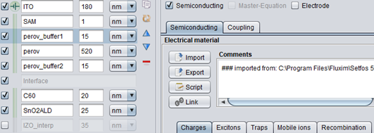
The solar cell stack in Figure 1 can be implemented in Setfos within the “layer structure” sub-tab of the “graphical input” tab (Figure 3). In the stack, “air_top” and “air_bottom” layers are included. The ITO and Cu layers are defined as “electrodes” (the cathode and the anode of the cell, respectively), while all other layers are defined as “semiconducting”.
2.2 – Step 2: Including the Optical Properties of Each Layer
To simulate measurements performed under illumination (e.g. Paios white LED or solar spectrum), an illumination spectrum needs to be defined. Light is incident onto the solar cell stack with a default 0° illumination angle and coming from the top (Figure 3b). The complex refractive index (or (n, k) data) of each layer is needed to correctly compute the light absorption profile and electron-hole generation rate across the stack. These data are available from the literature for a wide range of materials, while measurements for the specific layers used in the solar cell under study are recommended for accurate reproduction of the optoelectronic and spectral response of the device under light.
Figure 4a shows an example from the Setfos interface of the (n, k) data for the perovskite active layer used in this study. Figure 4b shows the steady-state generation profile obtained from an optical simulation of the stack considering the illumination spectrum in the inset (corresponding to the Paios LED used in the experiments under light in Figure 2b). The generation profile decreases rapidly reaching values close to 0 within the first 300 nm of the layer with only minor interference effects. Here, the internal quantum efficiency of the contact layers is set to 0 for a 1st order analysis, while their contribution to the photocurrent can be included at the refinement stage.
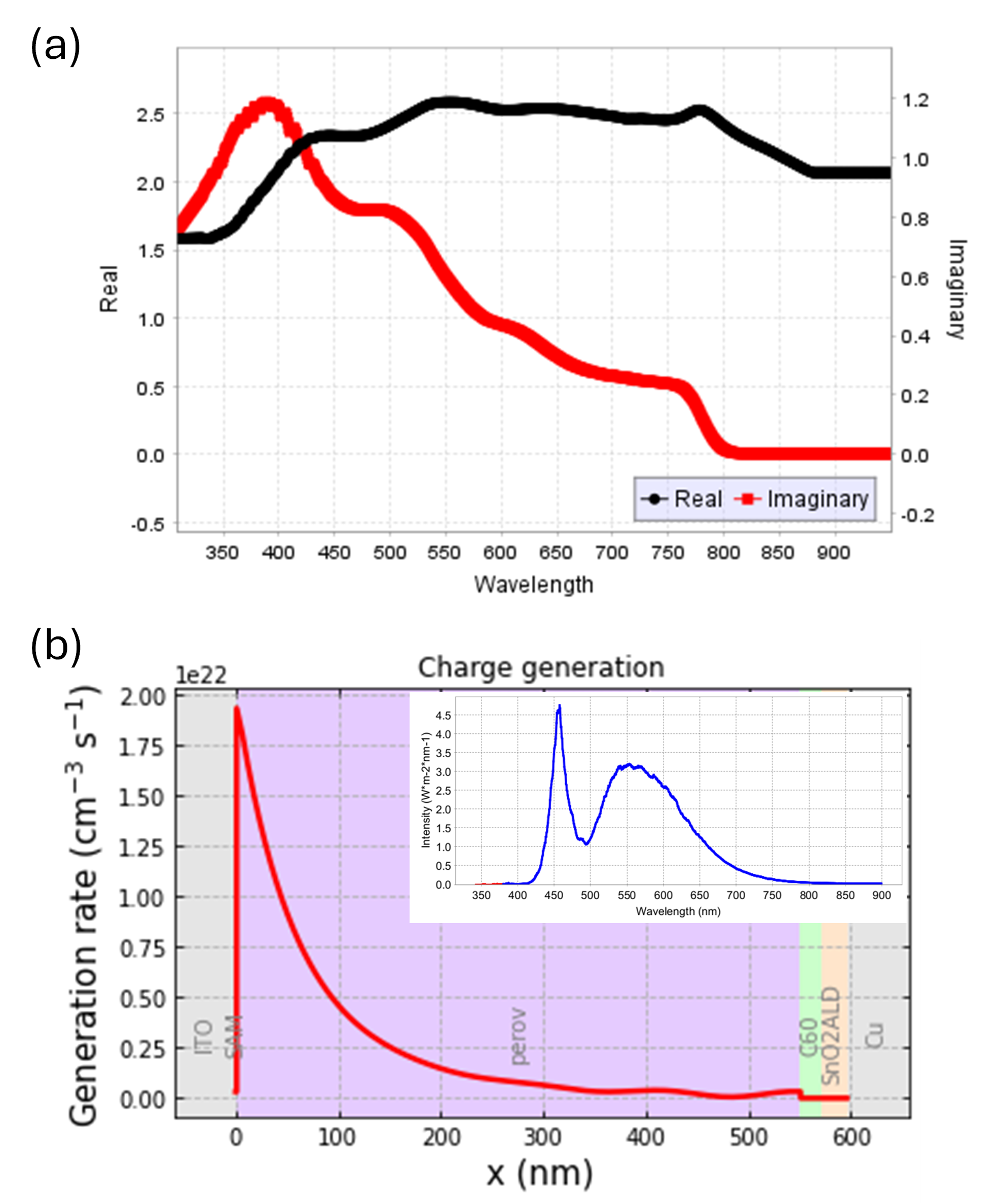
Figure 4 (a) Example of n, k data input in Setfos for the perovskite layer. (b) Photo-generation profile obtained from an optical simulation of the solar cell stack, using the illumination spectrum in the inset (Paios white LED).
2.3 – Step 3: Initial Guesses for the Electronic and Ionic Properties
Setfos allows the user to define each of the solar cell’s layers as electrodes or as semiconductors. For electrodes with ohmic injection properties, the work function or the electronic injection barrier of the material is required as the only input parameter.
For semiconducting layers, a range of properties needs to be defined.
These include the electronic energy levels, doping type and concentration, dielectric permittivity, effective density of states, electronic mobilities, trapping and recombination properties as well as the layer’s ionic properties (the latter being relevant to mixed ionic-electronic conductors). Reasonably good initial guesses can be taken from the literature for some of these parameters, as they are not expected to vary significantly among labs if the correct material composition phase and crystallinity are verified.
Other parameters (highlighted in italic above) are generally considered to be more sensitive to the preparation conditions, and their values may not necessarily match previously published data, despite following nominally analogous preparation procedures. It is therefore useful to refer to previous work (e.g. [12–16]) to define the initial guesses for many of the required input parameters. In some cases, literature offers a wide range of values, highlighting the need for measurements that are specific to the stack under study. This may not always be possible. An initial guess may then be required and, through comparison with experiments, these values can then be fitted to the data.
In this tutorial, we model ionic properties of the perovskite active layer by including one mobile cation species (representing the mobile halide vacancies) compensated by an equal density of immobile anions. We further assume here that ions are confined to the perovskite active layer. Additional points on the choice of initial guesses are discussed in Appendix B.
2.4 – Step 4: Refining the Mesh
To build the numerical problem from the physical system, Setfos implements mesh points for each layer using uniform spacing. Analysis of the simulation output in the bulk and at boundary layers can guide the optimization of the mesh structure. Specifically, a coarse mesh can be used in regions where limited variation in the solution quantities is expected, while a finer mesh can be adopted to carefully describe interfacial behavior, such as space charge layers. This is often needed for mixed ionic-electronic conductors that involve a large concentration of mobile defects. To do this, layers can be copy-pasted, linked to each other, and their thickness and mesh points adapted to the specific needs (“buffer layers” in Figure 5).
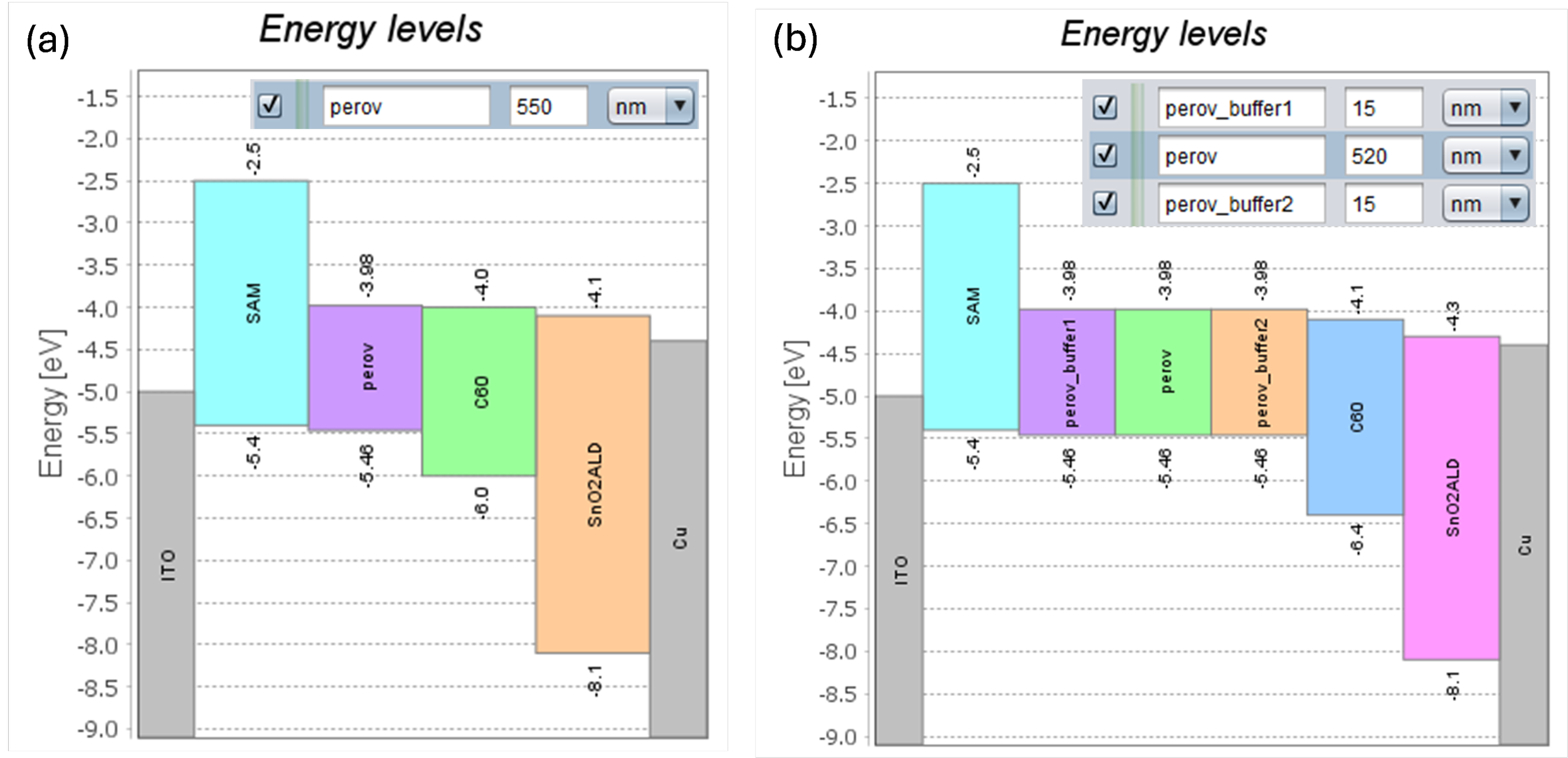
Figure 5. Energy level diagram showing (a) the initial guess of the perovskite solar cell device stack and (b) a refined version of the stack where thin buffer layers with improved resolution are included to describe the perovskite interfaces.
For the solar cell model used here, the mobile ion charge density profile at the perovskite’s interfaces for a simulation at equilibrium is shown in Figure 6. The results obtained with three different mesh spacing values for the buffer layers of the perovskite are compared. The data highlight that a too coarse mesh can lead to inaccuracies, while too fine mesh does not lead to significant improvement in accuracy, while potentially increasing the simulation time. In the example shown in Figure 6, a spacing of 1 nm is a satisfactory option.

Figure 6. Mobile cation density profile in the halide perovskite close to the interface (a) with the HTL and (b) with the ETL from simulations of the PSC under study at 0 V in the dark performed using three different mesh spacings in the “buffer layers”.
Note that adjustment of the mesh spacing should be carried out continuously when refining the model fitting to the experimental data, as the width of boundary layers depend on several input parameters as well as on the simulated bias conditions.
2.5 – Step 5: Series and Shunt Resistance
Non-idealities of the solar cells such as series and shunt resistance are not directly related to the nominal charge carrier physics of the device. These parameters can be included in the Setfos model as “external” parameters to the device stack. The value of the series resistance (Rs) and the shunt resistance (Rshunt) of the solar cell can be extracted, for example, by evaluating the real part of the impedance at high frequencies (for Rs) and at low frequencies (for Rshunt). Fitting a simplified equivalent circuit model to the experimental data can help determine accurate values for these parameters (see fitting performed using Characterization Suite in Figure 7).
In this analysis, we focus on impedance data, while other techniques (including time-domain methods) can also be used to extract these parameters. The model in Figure 7a shows a simple circuit that can reproduce the overall device response close to equilibrium, where an ionic resistor (Rion) and an electronic resistor (Reon) are introduced, as well as the interfacial (C1 and C2) and geometric (Cg) capacitors. Further simplifications to the circuit model can be made when fitting specifically the high-frequency and low-frequency response only. Figure 7b shows a simplified model where RHF is the parallel (∥) of Rion and Reon, while in the model of Figure 7c RLF = Reon. Finally, relatively low values of Reon can be assigned to shunt resistance (Reon ≈ Rshunt), especially for devices with selective contacts.
In some cases, the inclusion of the series resistance in the model can increase the simulation time, and it may be more convenient to evaluate its effect at the model refinement stage, if this is possible. For example, while the presence of Rs does not significantly affect the slow time-scale response of the device, accounting for Rs is generally necessary when evaluating the transient or frequency-domain response corresponding to fast time scales.1
1 Accounting for Rs can also be critical to reproduce j–V curves at large current densities. ↩

These values, along with the active area of the device and other relevant electrical parameters, can be included in the “Electrical circuit” section of Setfos, as shown in Figure 8.

Figure 8. Including the device area from the experimental specifications as well as series and shunt resistance obtained from model fitting to the impedance data within the electrical circuit option of Setfos in the Drift-diffusion settings -> General tab.
2.6 – Step 6: Dielectric and Ionic Response at Equilibrium
Investigating the impedance and capacitance-frequency (C-f) response of the solar cell at equilibrium is also a useful starting point to determine some of the dielectric and ionic properties of the device. [7,13]
From the trends in Figure 9 we highlight that:
- Nion influences the capacitance plateau at low frequency, as it determines the screening length in the perovskite. For large values of Nion, such capacitance tends to saturate, as it is limited by the capacitance associated with the contact layers.
- Both Nion and μion influence the transition frequency where the device capacitance drops when moving towards higher frequencies. This frequency relates to the time constant of space-charge polarization in the stack, which can be defined as the product of the ionic resistance (inversely proportional to the perovskite ionic conductivity, and therefore to Nion and μion) and the interfacial capacitance (sensitive to Nion, see above).[13]
- The value of εperov is relevant to the high-frequency capacitance, i.e., where no significant ionic redistribution occurs in the perovskite layer. The dielectric permittivity of other layers in the cell is also important for this fitting step (in the structure in Figure 1, the C60 layer is especially critical due to its low ε, despite it being only 20 nm thick). To further verify the dielectric permittivity values, it can be useful to analyze a set of devices with systematic layer-thickness variations.
By performing sweeps of these three parameters, it is possible to obtain a reasonably good fit, which reproduces the experimental impedance response visualized within a capacitance-frequency analysis or in a Nyquist plot (Figure 10). We discuss the slight underestimation of the experimental low frequency capacitance in the simulation in Appendix C.
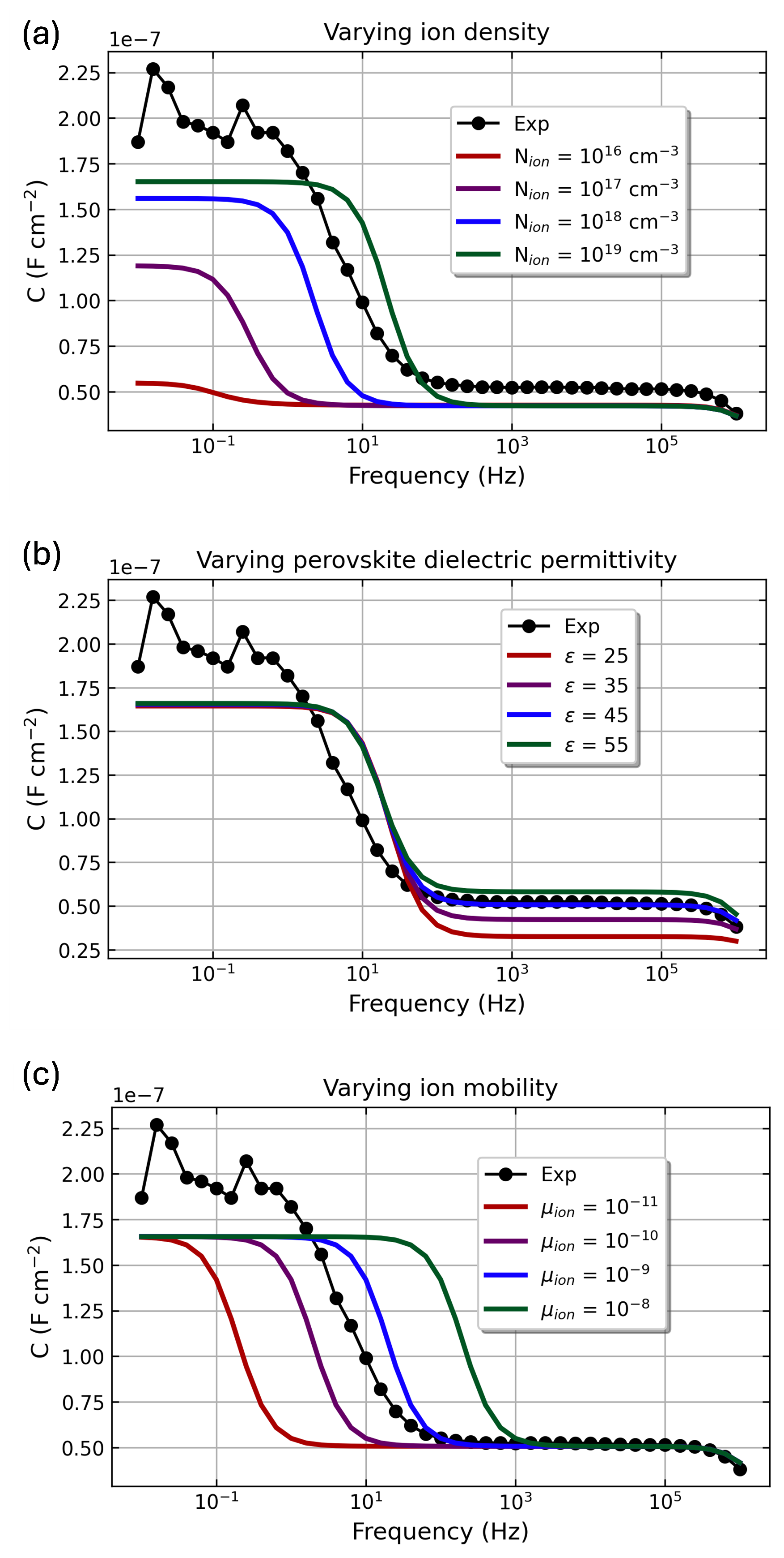
Figure 9. Capacitance-frequency plots illustrating the effect of different dielectric and ionic parameters on the model’s output response close to equilibrium. (a) The ion density influences the low frequency capacitance as well as the time constant of space charge polarization (both immobile anions and mobile cation densities are varied simultaneously). (b) Varying the perovskite’s static dielectric permittivity allows the fitting of the model to the high frequency geometric capacitance. (c) Varying the mobility of ionic defects in the perovskite influences the time constant of the ionic redistribution without changing the low and high frequency capacitance magnitude.

Figure 10. Fitted model reproducing the ionic and dielectric response of the solar cell. (a) Capacitance-frequency response and (b) Nyquist plot of the impedance at 0 V in the dark. The model uses a concentration of mobile ions of 1019 cm-3 an ion mobility of 4×10⁻¹⁰ cm-2 V-1 s-1and a relative dielectric constant of 45 for the perovskite layer.
2.7 – Step 7: Electronic Properties under Dark and Light
When it comes to evaluating the performance of the solar cell, and therefore the “photovoltaic quality” of the device, the J-V characteristics under light might be the most useful information for a scientist, but it may not be the most convenient starting point for implementing an accurate drift-diffusion model. Figure 11 shows the comparison of a simulated J-V obtained using the model developed so far and the experimental data collected with Paios. As we are evaluating steady-state j-V properties simulations should be compared with experimental data collected using slow enough scan rates. The data in Figure 11 were collected at 50 mV/s, an acceptable setting for this device architecture and measurement conditions (see minor variation in j-V response when using even lower scan rates on a similar cell in Appendix A). Given the good quality of the solar cell in this case, we assume that the collection efficiency at short-circuit is close to 100%. Therefore, the intensity scaling used in the simulation is adjusted to match the experimental short circuit current. In general, careful measurements of the illumination spectrum and irradiance are required to also include possible losses at short circuit in the model.
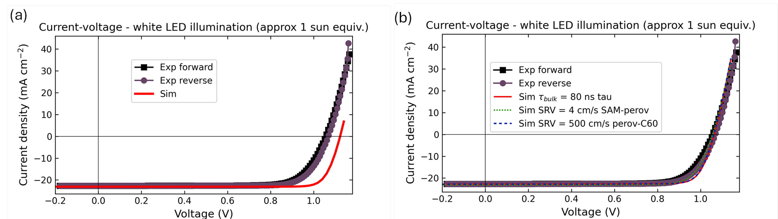
Figure 11. (a) Simulated steady-state j-V curves under simulated white LED illumination and using the initial guess for all electronic parameters. The simulation is compared to the experimental data. (b) Improved fitting of the model to the data is obtained by increasing the recombination rate either in the bulk or at the SAM/perovskite interface or at the perovskite/C60 interface.
To improve the understanding of which losses are dominant in the device, we include in the analysis j-V measurement and impedance spectroscopy measurements performed under dark conditions. We proceed and explore with Setfos the influence of different device parameters that lead to significant variation in response.
Figure 12 shows the simulated voltage dependent impedance obtained for the models used to reproduce the experimental j-V under light in Figure 11. Clearly, despite yielding similar j-V characteristics, the three models lead to very different sets of impedance spectra. The most striking observation is that dominant recombination at the SAM/perovskite interface leads to impedance values that can be associated with an apparent negative capacitance (inductive loop in Figure 12b, see ref. [11] for interpretation). This result indicates that such model may not be representative of the device behavior observed in the experiment, and we therefore rule out significant recombination happening at the interface with the SAM. On the other hand, both cases of dominant bulk recombination and dominant recombination at the perovskite/ C60 interface highlight voltage dependent low frequency features that qualitatively reproduce the experimental results. We therefore focus on these two mechanisms further.

Figure 12. Nyquist plots of the simulated impedance for the three models used also in Figure 11 for dominant recombination (a) in the bulk, (b) at the SAM/perovskite interface (c) and at the perovskite/C60 interface.
Additional insights can be gathered from dark j-V measurements. Here the voltage dependence of the current density can further refine the fitting of parameters directly associated with recombination loss mechanisms and of the other device parameters that this measurement is sensitive to.

This analysis allows us to: (i) improve the fitting of the contact and electrode layers’ energetics; (ii) compare the voltage dependence of different simulated recombination mechanisms to the voltage dependence of the overall experimental device current. Based on the parameter set yielding the best fit, we gather that recombination at the perovskite/C60 interface is likely the dominant loss in the measured device. While bulk recombination can still be significant, it does not appear to be dominant in these devices.
Figure 14 shows the summary of how the obtained model enables acceptable fitting to experimental current-voltage characteristics performed under dark and under light, as well as to the measured voltage dependent apparent capacitance-frequency data. For the j-V data, the full transient simulation following the same pre-bias and voltage scanning routine as in the experiment is presented. While some limitations to this analysis are set by the additional long time scale variations in device properties (see for example changes after bias of the dark J-V in Figure 14a, as well as partially reversible behavior in the measured impedance data in Figure 14c), the model is a useful starting point to explore further features of the device related to performance optimization and to degradation studies.

Figure 14. Results from the fitting procedure presented above, comparing experimental and simulated data: (a) transient j-V under dark, (b) transient j-V under light and (c) voltage dependent apparent capacitance data from impedance measurements and simulations.
2.8 – Step 8: Refining the Model
The steps presented above can facilitate the derivation of a baseline model, which already reproduces much of the optoelectronic response of the device. Other approaches are possible, whereby data collected using other time or frequency domain techniques can be used for the fitting procedure. Extending the range of techniques used in the fitting can ensure that the model is not just a “local minimum”, but it accurately represents the key features of the solar cell under study.
Further fitting analysis can also help refining the value of parameters that the techniques shown above show limited sensitivity to. For example, Figure 14 shows some inaccuracies in the fill factor of the current-voltage under light, as well as in its hysteresis properties. Longer time scale behavior mentioned above influencing the impedance measurements are currently not accounted for in the model. Finally, additional points regarding the model described above, including further experiment validating our simplified analysis, are presented in Appendix C.
Conclusions
This tutorial presents a possible procedure to implement a Setfos model reproducing experimental data collected for a single junction pin perovskite solar cell. By considering current-voltage measurements and impedance data collected using Paios, the key steps to obtain a digital twin of the solar cell are described. Further strategies to refine and to extend the model are discussed.
References
[1] M. M. Lee, J. Teuscher, T. Miyasaka, T. N. Murakami, and H. J. Snaith, Efficient Hybrid Solar Cells Based on Meso-Superstructured Organometal Halide Perovskites, Science 338, 643 (2012).
[2] M. T. Neukom et al., Consistent Device Simulation Model Describing Perovskite Solar Cells in Steady-State, Transient, and Frequency Domain, ACS Appl. Mater. Interfaces 11, 23320 (2019).
[3] T. Yang, G. Gregori, N. Pellet, M. Grätzel, and J. Maier, The Significance of Ion Conduction in a Hybrid Organic–Inorganic Lead‐Iodide‐Based Perovskite Photosensitizer, Angewandte Chemie 127, 8016 (2015).
[4] D. Moia and J. Maier, Ion Transport, Defect Chemistry, and the Device Physics of Hybrid Perovskite Solar Cells, ACS Energy Lett. 6, 1566 (2021).
[5] U. Aeberhard, Perovskite Solar Cell Simulation Tutorial with Setfos – Step-by-Step with Dr. Urs Aeberhard, https://www.youtube.com/watch?v=5FJ3pwY4KI0.
[6] M. Othman et al., Alleviating nanostructural phase impurities enhances the optoelectronic properties, device performance and stability of cesium-formamidinium metal–halide perovskites, Energy Environ. Sci. 17, 3832 (2024).
[7] O. Almora, I. Zarazua, E. Mas-Marza, I. Mora-Sero, J. Bisquert, and G. Garcia-Belmonte, Capacitive Dark Currents, Hysteresis, and Electrode Polarization in Lead Halide Perovskite Solar Cells, J. Phys. Chem. Lett. 6, 1645 (2015).
[8] A. Pockett, G. E. Eperon, N. Sakai, H. J. Snaith, L. M. Peter, and P. J. Cameron, Microseconds, milliseconds and seconds: deconvoluting the dynamic behaviour of planar perovskite solar cells, Phys. Chem. Chem. Phys. 19, 5959 (2017).
[9] D. A. Jacobs, H. Shen, F. Pfeffer, J. Peng, T. P. White, F. J. Beck, and K. R. Catchpole, The two faces of capacitance: New interpretations for electrical impedance measurements of perovskite solar cells and their relation to hysteresis, Journal of Applied Physics 124, 225702 (2018).
[10] D. Moia et al., Ionic-to-electronic current amplification in hybrid perovskite solar cells: ionically gated transistor-interface circuit model explains hysteresis and impedance of mixed conducting devices, Energy Environ. Sci. 12, 1296 (2019).
[11] D. Moia, Equivalent-circuit modeling of electron-hole recombination in semiconductors and mixed ionic-electronic conductors, Phys. Rev. Applied 23, 014055 (2025).
[12] J. Hidalgo, J. Breternitz, D. M. Többens, D. K. LaFollette, C. N. B. Pedorella, M.-J. Sher, S. Schorr, and J.-P. Correa-Baena, Br-Induced Suppression of Low-Temperature Phase Transitions in Mixed-Cation Mixed-Halide Perovskites, Chem. Mater. 36, 10167 (2024).
[13] D. Moia, M. Jung, Y.-R. Wang, and J. Maier, Ionic and electronic polarization effects in horizontal hybrid perovskite device structures close to equilibrium, Phys. Chem. Chem. Phys. 25, 13335 (2023).
[14] H. M. Pham, S. D. H. Naqvi, H. Tran, H. V. Tran, J. Delda, S. Hong, I. Jeong, J. Gwak, and S. Ahn, Effects of the Electrical Properties of SnO2 and C60 on the Carrier Transport Characteristics of p-i-n-Structured Semitransparent Perovskite Solar Cells, Nanomaterials 13, 3091 (2023).
[15] D. Turkay et al., Synergetic substrate and additive engineering for over 30%-efficient perovskite-Si tandem solar cells, Joule 8, 1735 (2024).
[16] A. Al-Ashouri et al., Monolithic perovskite/silicon tandem solar cell with >29% efficiency by enhanced hole extraction, Science 370, 1300 (2020).
Appendix A
Comments on the characterization of long-time behavior of perovskite solar cells
When testing a new device structure, and particularly its long-time scale behavior, it is essential to gather an overview of the following questions:
1) Are there any changes in device properties that are reversible but occur over time scales comparable or longer than the measurement time? If yes:
Designing appropriate and consistent pre-conditioning steps as an essential part of the characterization routine can guarantee repeatable measurements.
In practice, this may still be challenging, if such reversible processes occur over very long-time scales.
Figure 15 shows a pre-bias study that evaluates the effect of the pre-bias voltage and time for the cells investigated in the main text. The data highlight the sensitivity of the apparent cell’s performance to the pre-bias voltage as well as the minimum pre-bias time needed to obtain repeatable results.

Figure 15. Effect of pre-bias time and voltage on j-V measurements performed under light. For each panel, a pre-bias condition and j-V protocol is set and applied to the device three consecutive times. (a—d) Pre-bias at 0 V, (e—h) pre-bias at 1 V.
1) Is there any irreversible degradation occurring over time scales comparable with the duration of each measurement?
If yes:
A complete and reliable characterization of the device over “ionic time scales” may not be possible.
Repetition of fast measurements can be used to monitor the degradation process.
In the case study considered in the main text, the use of reference measurements that are applied intermittently throughout the measurement session can help ascertaining the extent of degradation in the device as well as identifying the stress conditions that may cause such degradation. For example, a separate test evaluating the capacitance-frequency response close to equilibrium before and after the j-V characterization shows negligible changes (Figure 16). This strategy may, however, not be sensitive to possible irreversible changes e.g. those affecting the electronic and coupled ionic-electronic response.

Figure 16. Impedance measurements performed in the dark at 0 V in between the sets of three consecutive current-voltage measurements (device with the same structure as the one presented in the main text). (a) Nyquist plot of the impedance. (b) Capacitance-frequency plot
Finally, for the cells studied in this work, only minor scan rate dependence was observed in the 5—500 mV/s range (Figure 17). This is consistent with the relatively large characteristic frequency associated with the ionic response of the solar cell in the capacitance-frequency plot. If pronounced changes in J-V vs scan rate were observed, simulations of steady-state J-V should be compared with measurements performed using low enough scan rates. Alternatively, fitting of simulated transient j-V can be the focus when adjusting and fitting the Setfos model, allowing the analysis of the complete scan rate dependence.

Figure 17. Scan rate dependent j-V measurements (reverse-forward protocol) performed under light (approximately 1 sun equivalent) following a pre-bias step of 100 s at 1.2 V.
Appendix B. Details on initial values for the drift-diffusion model
When implementing a complete Setfos model, not all required parameters may be available. In this study, based on general guidelines of material properties:
Representative values on the order of 1021, 1020 and 1019 cm-3 are explored for the effective density of states of organic semiconductors, oxide semiconductors and halide perovskites, respectively, whenever such values are not available from literature.
Electronic mobilities in the order of 10-1—102 cm2 V-1 s-1and 10-4—100 cm2 V-1 s-1are explored for inorganic and organic semiconductors. Further factors including doping and traps are important in defining the charge transport quality of contact and active layers.
For self-assembled monolayers (SAMs), a representation of the molecular properties may not be possible based on a traditional semiconductor picture. Here, we consider a layer of representative thickness and energy levels, with a large hole mobility referring to pseudo-intramolecular charge transport in the layer. As tunneling is currently not supported within Setfos, the HOMO level of the SAM is also tuned to values that allow efficient injection and extraction in the device, although this parameter can be tuned to reproduce electrical behavior further (indeed, measured values of the HOMO are on the order of 4.8 eV [16])
Different layers may be expected to contribute to the solar cell’s photocurrent, initial guesses for recombination parameters should be set accordingly. In the case of the PSCs investigated here, most of the extracted current is expected from photogeneration and extraction occurring in the halide perovskite active layer. Initially, fast recombination rate can be set for the contact layers, e.g. Shockley-Read-Hall recombination with capture lifetime in the order of nanoseconds.
Appendix C. Further model validation
The fitted model described in this document can be further refined by analyzing its validity across device structures. For example, here we investigate the ability of the model at predicting the response of the device upon changes in architecture. In Figure 18, the model is fitted to experimental data obtained for a solar cell with analogous structure as the one in Figure 1, but with a thicker C60 layer. The results show good agreement with experiments without the need to change any parameter in the model. Furthermore, this observation justifies the choice of using an undoped C60 layer in the model. Introducing a donor dopant in such layer would lead to a narrow space charge region and an increase in the low frequency capacitance, potentially improving the quality of the fit to the C-f data collected at 0 V in the dark (Figure 10). The fact that experimentally the low frequency capacitance scales with the reciprocal of the C60 layer thickness not only confirms that this layer largely limits such capacitance value, but also rules out the presence of a narrow space charge, which would be largely independent of the layer’s thickness. Further hypothesis that could be consistent with the large low frequency capacitance observed in the experiments include an even larger concentration of the mobile ionic defect, interaction of such defects with the transport layers (e.g. penetration of iodide in the C60 layer), contribution of a second mobile ionic defect to the ionic response of the solar cell.
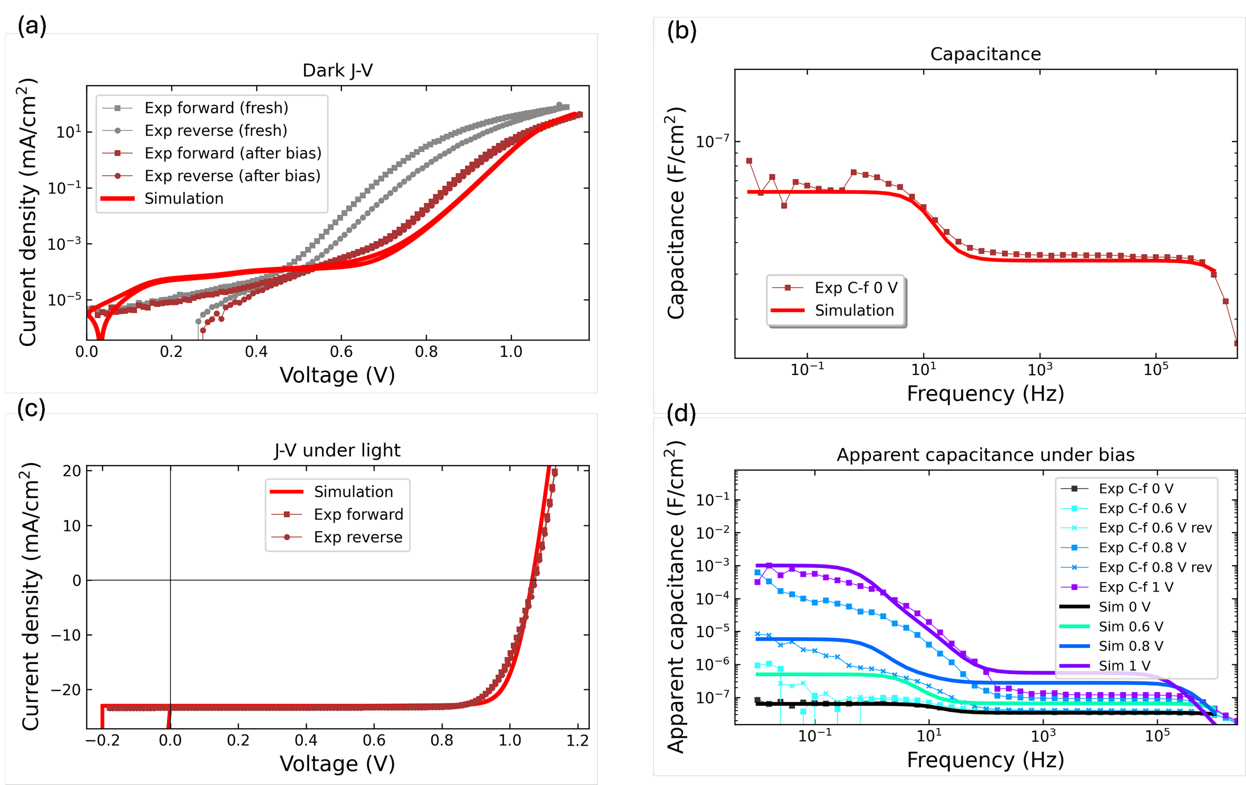
Figure 18. Comparison between experimental and simulated data collected for a solar cell with the same structure as the one shown in Figure 1 but with a 60 nm C60 layer. (a) j-V in the dark, (b) capacitance-frequency under dark at 0 V, (c) j-V under light, (d) voltage dependent apparent capacitance.