Research Paper — Far-field electroluminescence mapping and Setfos cavity fitting for directional micro-LED emission
Summary
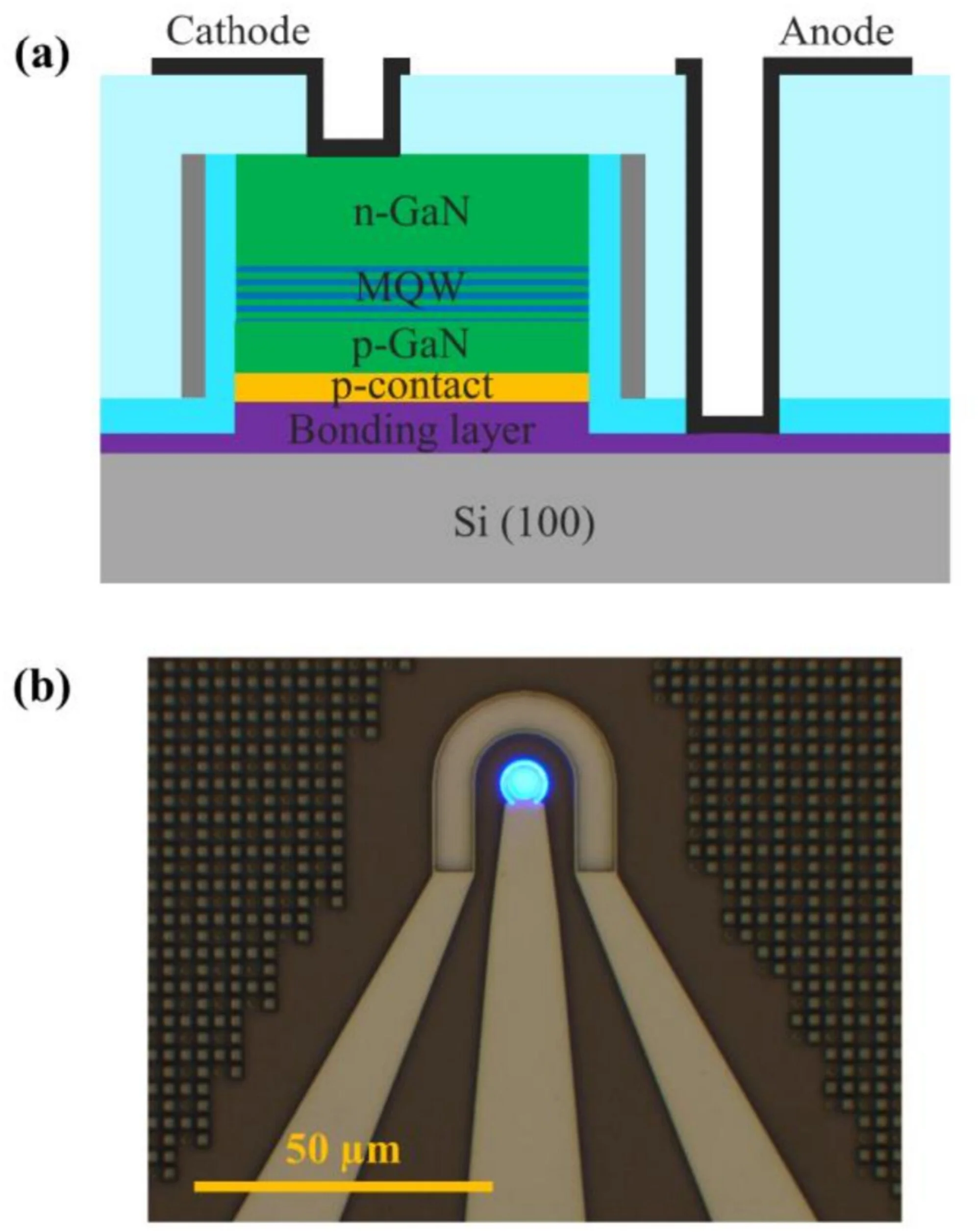
This study measures the angular dependence of far-field electroluminescence (EL) in InGaN/GaN LEDs and micro-LEDs (200 um down to 1.25 um) using Fourier-plane imaging with spectral filtering. The measured wavelength-resolved emission patterns are compared to 1D optical simulations, showing strong sensitivity of emission directivity and light extraction efficiency (LEE) to flip-chip cavity parameters, especially p-GaN and n-GaN thickness, and to total thickness variation introduced by wafer thinning. The authors also show that changes in the emission diagram can shift the apparent EQE maximum when the collection numerical aperture is limited, and they discuss when 1D cavity optics remains useful (down to about 5 um) versus when 3D-FDTD becomes necessary to capture sidewall effects (below about 5 um).
Publication details
Authors: Fabian Rol; Stephane Altazin; Nicolas Michit; Bastien Miralles; Clement Ballot; Bernard Aventurier; Paolo De Martino; Patrick Le Maitre; Julia Simon
Journal: Journal of the Society for Information Display
Year: 2025
Volume: 33
Pages: 1123-1134
DOI: 10.1002/jsid.2114
Fluxim tools used
Setfos was used for 1D optical simulations and fitting of far-field emission patterns.
Why it matters
Far-field EL provides a fast experimental handle to link micro-LED directivity and LEE to flip-chip cavity thicknesses and wafer-thinning driven total thickness variation.
Highlights that limited-NA EQE measurements can shift the observed EQE maximum when the emission diagram changes with injection and wavelength.
Gives a practical boundary for modeling choice, where 1D cavity optics remains informative down to about 5 um, while smaller pixels require 3D-FDTD to include sidewalls plus cavity effects.
Keywords
micro-LED; InGaN/GaN; far-field electroluminescence; Fourier-plane imaging; angular emission; emission directivity; optical cavity; dipole emission model; light extraction efficiency; wafer thinning; total thickness variation; flip-chip LED; p-GaN thickness; n-GaN thickness; AR/VR microdisplays; visible light communication; EQE collection angle; 3D-FDTD
FAQs
Q1: Why measure far-field EL with spectral filtering instead of only the full spectrum?
A: The angular pattern changes strongly with wavelength, so wavelength-resolved data makes cavity-model fitting much more sensitive and reliable.
Q2: Which layer thickness matters most for directivity and LEE in this flip-chip cavity?
A: The paper reports a stronger sensitivity to p-GaN thickness than n-GaN thickness, for both directivity and LEE.
Q3: When is 1D modeling no longer enough for micro-LED optics?
A: As pixel size shrinks below ~5 um, sidewall effects increasingly distort the far-field pattern, motivating 3D-FDTD approaches.