Here is how a Setfos simulation can help your development of LEDs and solar cells (with step by step tutorials)
Over the years, the pressure to speed up the development of new technologies has increased. Still, optimizing the stack of a solar cell or LED is a demanding and time-consuming experimental process. It requires fabricating a broad set of devices to cover the matrix of combinations of the relevant variables. Simulation can help researchers to speed up the development of their devices and to understand better the mechanisms that are governing the device operations.
Here, you can learn how our simulation software Setfos can support your research on solar cells and LEDs.
New Setfos Tutorials with Dr. Urs Aeberhard
To demonstrate the predictive power of Setfos we have produced two, step-by-step tutorials: Simulating a Solar Cell with Setfos and Simulating an OLED with Setfos.
Thanks to our colleague Dr. Urs Aerberhard, R&D Scientist at Fluxim and Guest Lecturer at the ETH, for both presentations.
Simulating an OLED with Setfos*
Simulating an Organic Solar Cell with Setfos*
Both tutorials are also available with Korean subtitles. Thanks to our colleague Moon Kang Heo (Technical Sales Engineer at Fluxim) for providing these. We will endeavor to add further languages in time.
Recent Results Obtained with Setfos
We’re always pleased that our research tools are being used to push the boundaries of what is possible with OPVs and LEDs. Here is the latest research from our customers who are using Setfos:
Enhanced hole injection assisted by electric dipoles for efficient perovskite light-emitting diodes

Xiangtian Xiao, Xiao Wei Sun & Wallace C. H. Choy, et al.
Communications Materials, 2020, 1, 81
https://doi.org/10.1038/s43246-020-00084-0
How do you improve the efficiency of your perovskite LEDs?
A strategy that has been recently proposed is to place a thin layer of MoO3 (Molybdenum trioxide) between the injection layer (HIL) and the hole transport layer (HTL).
MoO3 was not selected by a time-consuming trial-and-error experimental approach. The researchers performed simulations using Setfos which suggested using a material with a deep conduction band level.
The calculated profile of the electric field, the distribution of the carriers, and the profile of the charge recombination in the stack indicated that this interface layer would have enhanced hole injection. Before going to the laboratory, they have been able to predict uthat the fabricated perovskite LED would have higher current efficiency concerning the reference device, and this was then confirmed by the experiments. The improved charge balance helped to extend the device's lifetime.
Directional Polarized Light Emission from Thin‐Film Light‐Emitting Diodes
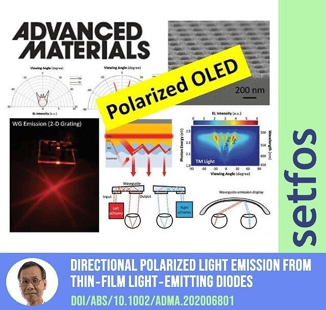
Xiangyu Fu, et al.
Adv. Mater. 2021, 33, 2006801.
doi.org/10.1002/adma.202006801
The authors are demonstrating highly directional polarized light emission from nanostructured organic and perovskite Light-Emitting Diodes (LEDs).
These LEDs could be used in innovative 3D displays using waveguide emission to project the images to the user's eyes for virtual reality (VR) and augmented reality (AR).
Prof. Franky So and colleagues fabricated TE polarized OLEDs and pero-LEDs using corrugated ITO electrodes.
To obtained waveguide-only emission, the device architecture had to be thoroughly optimized to extract the waveguided mode while suppressing emission from the air, TM waveguide, and SPP modes. Importantly, this work demonstrates also that perovskite emitters are perfect candidates for waveguide emission thanks to the high refractive index and, therefore, a high TE waveguide distribution.
Setfos helped them designing the devices before the actual experiments.
Our simulation software was used to perform a thorough dissipation power analysis to visualize the TE waveguide modes, but also to optimize the layer thickness and refractive index of the OLED and pero-LED.
Efficient Double- and Triple-Junction Nonfullerene Organic Photovoltaics and Design Guidelines for Optimal Cell Performance

Yuliar Firdaus, Thomas D. Anthopoulos, et al.
ACS Energy Lett. 2020, 5, 12, 3692
doi.org/10.1021/acsenergylett.0c02077
Researchers at the KAUST Solar Center (KSC) have developed guidelines on how to design an optimal Organic Solar Cell (OSC).
They focused on non-fullerene multijunction solar cells that, despite the broader light absorption, still suffer from low Power Conversion Efficiency (PCE).
Before the device fabrication, the team of Prof. Thomas Anthopoulos and collaborators used Setfos to understand which are the main factors that limit the efficiency of a multijunction solar cell.
They discovered that, aside from the clear requirement of matching the absorption spectra of the different materials, having low bimolecular recombination and high mobility on the front-cell was the key. Based on the knowledge given by the simulation, they fabricated multijunction organic solar cells which are among the highest efficient devices reported to date. On double-junction OPVs they achieved a conversion efficiency of 16.5%
Could Setfos Advance Your Research?
What researchers are saying about Setfos
“We have extensively used both SETOS and LAOSS in our recent endeavour to model large-area OPV and OLED devices. The intuitive workflow of both software packages allows us to quickly try out new ideas before realising them experimentally.”
Dr. Ardalan Armin, Ser-SAM group, Department of physics, Swansea University
"Our team purchased the optical and electrical modules of Setfos in July 2020. The operation interface of the software is intuitive, friendly, and easy to operate. The software itself contains rich information within a large material database. In the OLED device simulation process, we can simulate the emission spectrum of OLED, and simultaneously the recombination zone of charge transfer and drift spread. It can also help us to modify the design of device structure and can effectively analyze and improve the OLED device efficiency. The results calculated by Setfos could be served as a good reference point for our scientific research. We would highly recommend you consider Setfos as the option."
Dr. Ding, OLED simulation team, Ningbo Research Institute, China
"Setfos has been an asset to our research capability in CSIRO Energy and a key tool in our research and assessment of next-generation thin-film photovoltaics, in particular, organic and perovskite solar cells. One of the key points of differentiation – and a clear attraction – has been the flexibility of the system and the ease in which user-defined experiments can be created. Our Team has appreciated the interaction with Fluxim and realised this has been much more than a transactional experience – we’ve formed a real partnership between developers and researchers.."
Dr. Gregory J. Wilson, Research Group Leader, CSIRO Energy, Newcastle, Australia
“Setfos is a very powerful simulation tool developed by Fluxim predominantly in the field of OLED and OPV researches. We are heavily dependent on this simulation tool regarding our research activities in OLED and OPV as evident in our publications. Setfos not only helps us in optimizing the device structures prior to device fabrication experimentally but also assists in analyzing the device physics through the simulation on the contribution of the various optical modes in the device as well as estimating the important parameters such as color coordinates, angular dependence, reflection and transmission co-efficient etc. Undoubtedly, Setfos takes an important role in the progress OLED and OPV research.”
Prof. Shun-Wei Liu, Department of Electronic Engineering & Organic Electronic Research Center, Ming Chi University of Technology, Taiwan
The new 2021 Setfos brochure can be downloaded here

We’re always improving what Setfos can do. Download the latest Setfos brochure and read about how it can be used to design LEDs & solar cells based on organic semiconductors, perovskites, and quantum dots.
Four different modules to simulate light emission, absorption, scattering, and charge transport.
Multithreading ensuring high-speed computation.
Fitting and optimization algorithms.
Outstanding track record: 15 years in industry and academia resulting in over 200 scientific publications. Sound materials & device models have been successfully validated by dedicated experiments.
The Setfos-Paios Integration gives access to combined characterization/simulation in DC, AC, and transient regimes
About Setfos
Setfos is an advanced simulation software used by R&D scientists to rapidly model, analyze and improve their devices. Setfos was initially developed as a tool for modeling light-outcoupling in OLED devices (that was way back in 2004). Since then we’ve developed software to aid the development of LEDs and solar cells and more recently batteries. You can view the full Setfos applications here.
Setfos has 4 modules:
Absorption, Drift-Diffusion, Advanced Optics, and Emission.

What devices can be Designed, Analyzed and Optimized with Setfos?
Photovoltaic Devices
Organic PVs
Perovskite PVs (including tandems)
Inorganic PV
Photodetectors
Light-Emitting Devices
Organic LEDs
Perovskite LEDs
Quantum Dot LEDs
QD-Films for LCDs