
Characterization Techniques For Organic and Perovskite Solar Cells
What this tutorial helps you do
- Choose the right mix of DC, transient, and AC measurements for perovskite and organic solar cells
- Link each method to the physical parameters it can reliably constrain
- Avoid common misreads caused by hysteresis, ions, interfaces, and RC effects
Key takeaways
- JV alone rarely identifies the dominant loss mechanism
- Transient methods add transport, trapping, and recombination time scales
- AC methods separate processes by time constant but need careful interpretation in perovskites
- Cross-check extracted parameters with a physics-based device model
Scientific note: This tutorial is based on Neukom et al. (2018) and the accompanying Supplementary Information. Paper
Perovskite solar cells (PSCs) are an emerging class of photovoltaic devices that stand out for their high efficiency and low manufacturing costs. These cells use a perovskite-structured compound—typically a hybrid organic-inorganic lead or tin halide—as the light-harvesting layer. Their excellent light absorption and charge transport properties have enabled rapid gains in performance, with laboratory efficiencies exceeding 25% in single-junction devices and even higher in tandem configurations. Many record-holding devices used these techniques — see the list.
Unlike traditional silicon solar cells, PSCs can be manufactured using low-temperature, solution-based techniques such as spin coating or printing. This simplifies production and reduces energy input, making them attractive for scalable and cost-effective solar energy applications. However, challenges such as limited long-term stability and the presence of toxic materials like lead still need to be addressed through further research.
Perovskite solar cells (PSC) and Organic Solar Cells (OPV) are promising candidates for the next generation of thin-film photovoltaics, but also as components of tandem devices when coupled to crystalline silicon, organic semiconductors, or CIGS.
Developing a physical understanding of mechanisms governing the operation of perovskite thin-film solar cells is much more demanding than for silicon solar cells. The charge transport in silicon solar cells depends only on the diffusion of one species of charge carriers (minority carriers). In thin-film solar cells, the electrode’s work function creates a built-in electric field, which assists the charge transport by establishing a drift-current. The electron and hole densities vary spatially and both species are influencing the characteristics of the solar cell.

Characterizing and quantifying charge transport in p-i-n structures requires measuring the electron and hole mobilities, the recombination coefficient, the built-in potential, charge injection barriers, and several parameters associated with charge trapping. As these parameters are entangled, conclusions from only one experiment are error-prone. Only the combination of different measurement techniques that combine steady-state, transient, and frequency-domain experiments can give a reliable insight into device physics.
This tutorial presents different optoelectronic characterization techniques that can be used on organic and perovskite solar cells. To help you visualize the impact of the non-idealities of the solar cell on the selected type of measurement, we also simulated several loss mechanisms and a reference case named “base case” (Figure 1). For each measurement, each loss mechanism is compared qualitatively with the base case.
Table 1 aims to guide you in the choice of the combination of measurement techniques based on the device parameter you intend to analyze or, conversely, it shows the properties that can be derived by the specific technique.

Try data fitting and device simulation in Setfos
Fit measurement data and test physics-based models before your next experiment.
Measurement techniques and extractable physical parameters in thin-film solar cells
| PROPERTY | DC MEASUREMENTS | TRANSIENT MEASUREMENTS | AC MEASUREMENTS | |||||||||
|---|---|---|---|---|---|---|---|---|---|---|---|---|
| Dark-JV | Light-JV | CELIV | OCVD | TPV | DLTS | TPC | CE | IS | CV | IMPS | IMVS | |
| VOC, JSC, FF, MPP, PCE | X | |||||||||||
| Ideality Factor | X | X | X | X | ||||||||
| Mobility (μ) | (X) | X | ||||||||||
| Doping (Na) | X | (X) | X | |||||||||
| Relative Permittivity (εr) | X | X | X | |||||||||
| Charge Carrier Lifetime | X | X | X | |||||||||
| Density of States (1/cm3/eV)* | X | X | (X) | |||||||||
| Trap Depth (eV)* | X | X | ||||||||||
| Charge Density (1/cm3) | X | X | X | (X) | ||||||||
| Built-In Voltage (Vbi) | (X) | X | ||||||||||
| RC-Effect | X | X | ||||||||||
| Charge Transport Time | (X) | X | ||||||||||
| Ion density/mobility | X | X | ||||||||||
Table description. Overview of DC, transient, and AC measurement techniques commonly used to extract physical parameters in thin-film and perovskite solar cells. An “X” indicates that the parameter can be directly or reliably obtained using the corresponding method.* requires temperature-dependent data.


Common pitfalls in perovskite measurements
- JV hysteresis can change PCE with scan rate and direction
- Mobile ions can distort DC and low-frequency AC interpretations
- RC effects can shift time constants and bias extracted mobility
- Interfaces can mimic bulk recombination signatures
- Single-measurement conclusions are often non-unique
Need help choosing the right measurements
Tell us your stack and what you want to learn. We will suggest a minimal measurement set and what each measurement can and cannot conclude.
Send your question1. DC Measurements
With direct-current (DC) measurements for perovskite thin-film solar cells, we refer to the electrical steady-state characterization of solar cell devices. The measurement can be carried out with the device in dark conditions or under various illumination intensities. DC measurements are the most common sources of information for all perovskite photovoltaics.
1.1 Current-Voltage (JV) characteristics
(Voc, Jsc, FF, MPP, PCE)
The collection of the JV-curve is the default characterization technique for a solar cell. Conventionally, it is obtained by performing a current−voltage (J−V) sweep under 1−sun (1000 W m−2 illumination at AM1.5G). The result is a curve, which crosses the x−axis (voltage) at the point called the open−circuit voltage (Voc) and the y−axis (current) at the point called short−circuit current (Jsc). As clear from the figure below, the solar cell JV characteristics are not squared. This indicates that the power extracted from the device is less than the product of Voc and Jsc. Instead, one has to determine the so−called maximum power point (MPP). The MPP is the point at which voltage and current result in the maximum power (Pmax) that can be obtained by the device. The voltage and current at the MPP are not practical parameters to characterize a solar cell.
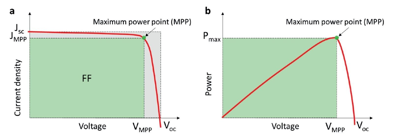
(a) typical JV curve of a perovskite solar cell characterized under constant illumination. (b) power output as a function of the voltage.
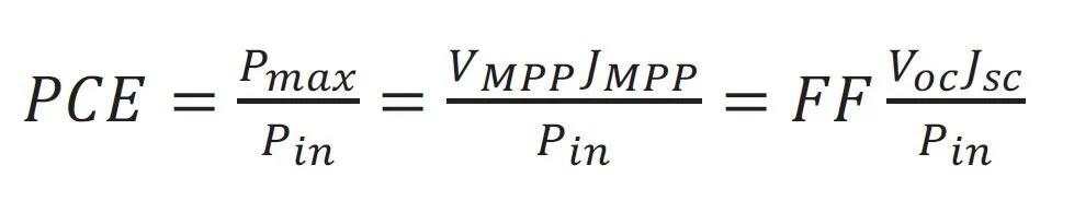
Instead, one can introduce a geometrical factor (the Fill Factor or FF) to relate these parameters to the Voc and the Jsc. The FF is the power available at the maximum power point divided by the Voc and the Jsc. Bartesaghi et al. [Bar15] showed that the FF in organic solar cells is mainly determined by the ratio of charge extraction versus charge recombination. With these parameters, it is possible to quantify the power conversion efficiency (PCE). Altogether FF, Voc, Jsc, and PCE are the most commonly used performance metrics to characterize solar cells.
This way of determining the PCE of a perovskite solar cell is independent of the J−V scan direction. It works as long as the measured solar cell is in quasi-steady-state conditions. This requires the device to be in equilibrium under each applied potential during the measurement. However, this is not always the case for perovskite solar cells (PSCs). Depending on the J−V scan direction, the result of the measurement is most of the time not unique. This phenomenon is called J−V hysteresis. With hysteresis, the PCE depends additionally on the scan rate. Hysteresis−free curves are obtained when the scan is performed either very fast or very slowly, but only in the latter case steady−state conditions can be achieved for the proper measurement of the PCE. Today, a broad consensus has been reached that the motion of ions (and their vacancies) in the perovskite is to blame for the J−V hysteresis. The case ‘extraction barrier’ shows a pronounced S-shaped JV curve. S-shapes are often associated with effects at the interfaces. A non-aligned contact leads to a lower built-in and Voc. The JV curve is therefore shifted to the left. The open-circuit voltage increases in the case of‘ low mobilities’. With Langevin recombination, lower mobility leads to less recombination and thereby to an increase in open-circuit voltage. We note that several of the investigated cases lead to a similar modification of the JV-curve harming the FF compared to the base case, as shown in Figure 3. Therefore, by measuring JV-curves only it is hardly possible to identify which non-ideal case is present. In the case ‘high Langevin rec.’, the Voc and the FF are reduced. A very similar effect occurs in the case of "deep traps". ‘Shallow traps’ have no impact on the steady-state Jsc current in our model, but reduce the FF. The shunt resistance in this example has only a minor effect on the JV curve. The FF is slightly reduced. A change in series resistance leads to a change in the current slope in the forward direction and to a lower FF. Charge carrier doping can be very detrimental to the efficiency of solar cells as doping introduces an extra charge inside the bulk that screens the electric field. In the case of‘ low charge generation’ the short-circuit current is decreased as expected and the FF is increased.
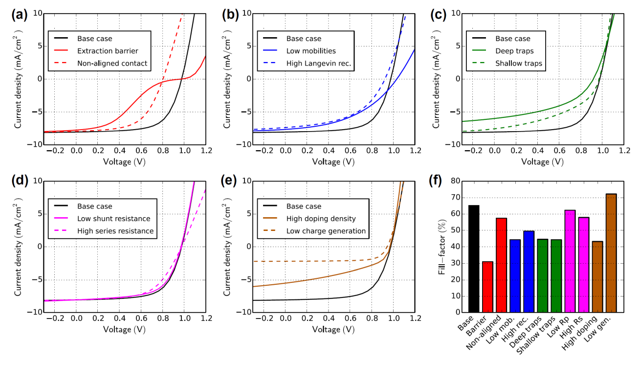
Figure 3: Jv-curve simulations for all cases defined in Table 1. (f) The bar-plot shows the fill-factor of all simulated cases. all the described cases impact the fill-factor.


1.2 Dark JV characteristics
Aside from that can be extracted from the JV characteristics under AM1.5G, the current-voltage (JV) curves measured in the dark gives complementary information. The recombination type (so-called ideality) and the shunt resistance can be obtained from the characteristics of the cells when measured in dark.
In classical semiconductor physics, the JV characteristics of a p-n junction in the dark are described by the Shockley equation.

The ideality factor is usually a factor between 1 and 2. In p-i-n solar cells, an ideality factor of 1 is interpreted as bimolecular recombination, a value near 2 is a signature of SRH recombination.
The ideality factor is a measure of whether the recombination type is SRH (nid = 2) or bimolecular (nid = 1). We however want to point out that the concept is based on a single zero-dimensional device model. In a real device, the charge carrier distribution varies in space and energy which can influence the ideality factor even if no traps are present. In organic solar cells, the photocurrent jph can depend on the voltage due to Onsager-Braun dissociation of excitons into free carriers [Mih04]. In perovskite solar cells the concept of ideality factor is controversial since the recombination at the interfaces has a larger influence than SRH or bulk recombination on the extraction of the ideality factor. [Cap20] The ions in perovskites cause misinterpretations of the ideality factor measure in DC conditions since these are voltage-dependent measurements. For this reason, Bennett et al. [Ben21] proposed an alternative measurement of the ideality factor based on impedance spectroscopy.
Where j is the current density, js is the dark saturation current density, q is the unit charge, V is the voltage, nidd is the dark ideality factor, kB the Boltzmann constant and T the temperature. The ideality factor is usually a factor between 1 and 2. In p-i-n solar cells, an ideality factor of 1 is interpreted as bimolecular recombination, a value near 2 is a signature of SRH recombination.

Figure 3.2: Schematics of the dark and light current-voltage curve in linear and logarithmic scale. The parameters mentioned in the text are indicated.
The ideality factor can be easily calculated from the JV characteristics. For positive voltages bigger than the thermal voltage the exponential term dominates and the ideality factor is calculated from the slope of the logarithm of the dark current density versus applied voltage:

In the reverse direction, the diode is ideally blocking and the current is determined by the parallel resistance. A low parallel resistance is usually caused by shunts in the device and can also be non-Ohmic. Very high trap densities can however also lead to an increase in the reverse current. In forward direction charge carriers are injected and recombine.
The case ‘low shunt resistance’ (Figure 3d) shows a much higher reverse current. The parallel resistance can be determined accurately from the differential resistance in reverse.

Figure 3. Dark JV-curve simulations for all cases in Table 1. (f) Dark ideality factors are extracted using Equation (2).
In the case, of “non-aligned contact” (a), the exponential current increase is shifted to a lower voltage due to the smaller built-in voltage. Low mobility leads to a smaller forward current as observed in Figure 3(b). The slope of the current in the exponential regime is similar in all cases except for the case of ‘deep traps’ (c). The dark ideality factor, extracted using Equation (2), is around 1 for most cases and around 2 for the case “deep traps”.
One of the main downsides of the dark-ideality factor is that it is affected by series resistance and parallel resistance, making it difficult to attribute changes in the measured ideality factor to changes in shunt or series resistance on one and recombination on the other hand. This causes results to disagree with the light ideality factor (presented in the next section).
To overcome the issues of resistance with the extraction of the dark ideality factor, one can obtain it from the Voc trend obtained from JV measurements carried out at increasing light intensity.
Measuring the open-circuit voltage versus the light intensity can be used to extract the light ideality factor. The ideality factor is a measure of whether the recombination type is SRH (nidL = 2) or bimolecular (nidL = 1). In an ideal device, the light ideality factor nidL is identical to the dark ideality factor nidd from dark JV-curves. In real devices, dark and light ideality factor can deviate. Since the light ideality factor is not influenced by the series resistance it is easier to analyze. An expression for the open-circuit voltage Voc is obtained by setting the current to zero in the Shockley equation (Equation (1)):
1.3 Light-dependent JV (ideality factor extraction)


where nidL is the light ideality factor, kB the Boltzmann constant, T the temperature, q the unit charge, jph the photocurrent and js the dark saturation current. Under the assumption that the photocurrent scales linearly with the light intensity and jph/js >> 1, the light ideality factor is calculated according to:

Where L is the normalized light intensity. In Figure (4)(f), the light ideality factor is shown, calculated from the average slope of the Voc versus the light intensity according to Equation (5). The base case has an ideality factor of exactly one. Apart from the case ‘low shunt resistance’ and ‘deep traps’ the ideality factor is around 1. If the recombination pre-factor is increased (b), the Voc is lower, but the Voc-slope remains constant. In the case of ‘deep traps’ (c), the slope (Voc vs. L) is significantly steeper leading to an average ideality factor of 1.8. In the case ‘low shunt resistance’ (d), the Voc collapses at lower light intensity and the calculation of an average ideality factor does not make sense.

Figure 4. Simulation of the open-circuit voltage dependent on the light intensity for all cases in Table 1. (f) Light ideality factors obtained from the simulation results – an average is used.
References:
Try data fitting and device simulation in Setfos
Fit measurement data and test physics-based models before your next experiment.
2. Transient Measurements
The measurement of a transient entails the recording of the response of an electrical parameter (like current or voltage) over time after the application of a stress. The stress can be illumination, voltage bias, or a combination of the two.
2.1 Charge extraction by linearly increasing voltage (CELIV)
Charge Extraction by Linearly Increasing Voltage (CELIV) is a popular technique to estimate charge carrier mobilities in organic and perovskite solar cells. Various types of CELIV experiments exist and will be described below. They are based on the same key idea: a displacement current generated in a material by an external trigger can be recorded and used to extract significant information about the material itself.
The important information we can extract from a CELIV experiment is the mobility of the charge carriers.
Figure 5 shows the principle of CELIV schematically. A linearly increasing voltage in reverse direction is applied to the device V(t) = A⋅t, where A is the ramp rate. The linearly changing voltage induces a constant displacement current density jdisp, which is calculated according to

where S is the device area, Cgeom is the geometric capacitance, ε0 is the vacuum permittivity, εr is the relative dielectric permittivity and d is the active layer thickness. The series resistance and the geometric capacitance can be evaluated from the initial current rise and the later constant displacement current, respectively.
If charge carriers are present in the device, they are extracted and lead to a peak in the transient current (jmax). According to the time of the current-peak (tmax) the charge carrier mobility can be estimated.

Figure 5. Schematic illustration of a photo-CELIV experiment. The linearly increasing voltage extracts charge carriers and leads to a peak (jmax) in current. The charge carrier mobility is calculated using tmax.
Various modifications of the CELIV technique exist:
In Dark-CELIV the ramp is applied in the dark and without an offset voltage. Usually, then only the constant displacement current is expected. In the special case of doping, however, mobile equilibrium carriers are extracted, leading to an overshoot.
For Injection-CELIV a positive offset voltage is applied so that an injection current flows before the ramp. During the ramp, the current reverses and shows a peak before reaching the displacement plateau.
In Photo-CELIV the device is illuminated and an offset voltage around Voc is applied prior to the ramp so that no current flows. The ramp then extracts the photogenerated carriers showing a peak on top of the displacement current plateau. While we wait for steady-state before starting the ramp, other groups are working with short laser pulses generating many charges instantaneously, before the ramp starts. We find, however, that deviations from zero of the current before the ramp can influence the extracted parameters strongly.
MIS-CELIV is basically an Injection-CELIV experiment performed on a MIS-device. The difference is that charges are injected by a positive pre-bias, but no equilibrium current can flow, so the CELIV current starts at zero, making it easier to interpret.
In Delay-time-CELIV the Photo-CELIV measurement is performed several times with a varying delay time between the light pulse and the voltage ramp. During the delay time, charges can recombine and fewer charges are extracted. The technique can therefore be used to study recombination kinetics. Keeping the voltage at a constant value during the delay time, however, can lead to counter-injection. OTRACE therefore adapts the voltage according to the TPV decay during the delay time, such that the current is always zero prior to the ramp.
In Reverse-CELIV a positive voltage ramp is applied, starting at a negative bias. The current then rises to the displacement current plateau, and when injection sets in, increases rapidly. This technique is only interesting in MIS-devices or strongly degraded cells.
Here, we will describe in details Dark-CELIV and Photo-CELIV:
Dark-CELIV
(relative permittivity and doping)
Dark-CELIV can be used to extract the relative dielectric permittivity and estimate the doping density. A negative voltage ramp is applied to the device in the dark. The relative dielectric permittivity can be calculated from the displacement current jdisp by rearranging equation (5):

The doping density of the device can be estimated by integrating the current. The charges on the electrodes (Q = C⋅V) need to be subtracted. The doping density can be estimated according to

where d is the active layer thickness, q is the unit charge, tramp is the time when the ramp ends, j is the current, Cgeom is the geometric capacitance, V is the applied voltage and S is the device area.
Figure 6 shows the simulation results of dark-CELIV using the cases defined in Table 1 (section 2). The only device that shows a current peak is the case with a high doping density. The homogeneous immobile doping induces oppositely charged carriers, which are mobile and can be extracted by CELIV. The parallel resistance leads to an increase in current over time. In such a case neither the integration of the current nor the estimation of the electric permittivity works.

Figure 6. Dark-CELIV simulations of all cases in Table 1. The ramp starts at t = 0 with a ramp rate of 171 V/ms. (f) The bar plot shows the extracted charge carrier density.
In the other cases mostly RC-effects are observed. We apply Equation (6) to the simulation results. The relative permittivity is obtained with an error of less than 1% in all cases except ‘low shunt resistance’ and ‘high doping density. Please be aware that the capacitance of the device can change over time, for example, due to mobile ions as observed in perovskite solar cells. In such a case the calculation of the relative permittivity is less accurate.
In the case of doping density extraction, it is important to note that not all charge carriers can be extracted due to the finite ramp-time. The doping density extracted from dark-CELIV should therefore be interpreted as a lower limit for the doping density. We recommend to perform the experiment with varying the ramp-rates and to use the highest density value.
An alternative method to extract the doping density from dark-CELIV currents was presented by Sandberg et al. analyzing the shape of the current-decay, based on the Mott–Schottky formalism [San14]. Seemann and co-workers demonstrated the evolution of unintentional doping during device degradation using dark-CELIV measurements [See10].
Photo-CELIV
(mobility, recombination coefficient)
In photo-CELIV, free charge carriers are generated by a light pulse prior to the voltage ramp. These charges are subsequently extracted by the applied voltage. The extracted charge carriers lead to a current overshoot superimposed on the displacement current. As a light source either a light emitting diode (LED) or a laser is used. When the charge carriers are extracted from the bulk they create a current overshoot Δj = jmax-j0.
The time where the current peaks (tmax) can be used to calculate the charge carrier mobility by:


where μ is the charge carrier mobility, d is the active layer thickness, A is the ramp rate, tmax is the time where the current peaks, jdisp is the displacement current and Δj is the peak current minus the displacement current. The factor 1 + 0.36⋅Δj/jdisp in the formula is an empirical correction accounting for the redistribution of the electric field.
The analytical approach is based on a simple model that considers one charge carrier type to be mobile and the other one to be static. The initial distribution of the charges is considered to be uniform in the bulk and diffusion is neglected. These approximations are usually inadequate to describe thin film devices so the formula (Equation 8) obtains the charge carrier mobility with an accuracy of a factor of 4. The RC effects lead to a strong underestimation of mobility. In such a case, it is advised to increase the thickness of the transparent conducting oxide (TCO) and metalize the TCO stripes. This effectively reduces the series resistance and thereby the RC time constant. Furthermore, it is advised to use devices with a small area leading to a small capacitance and a low RC time.
Figure 7 shows the photo-CELIV response for the cases defined in Figure 1. All devices show a current overshoot with peak times ranging between 2 and 6 μs. Figure 7(f) shows mobilities calculated using Equation 8. The extracted mobility agrees within a factor of 2 with the input electron mobility (grey line), except for the case with the high series resistance. It leads to a slower charge extraction and to an underestimation of the mobility. In the case of low mobility (Figure 7(b)) the current extraction is slower and the extracted mobility is lower. Traps significantly influence the charge extraction as visible in Figure 7(c). Deep traps create additional recombination channels (SRH), therefore less charge is extracted. Shallow traps, however, save charges from recombination. Therefore, more charge is extracted and the apparent mobility is lower.
2.2 At Voc conditions (OCVD, TPV)
Figure 7. Photo-CELIV simulations for all cases in Table 1. The light is turned off at t = 0 and the voltage ramp starts at t = 0 with a ramp rate of 100 V/ms. The voltage offset prior the ramp is set such that the current is zero at t < 0. (f) The bar plot shows the charge carrier mobility calculated from the peak position (tmax) using Equation (9). The grey lines indicate the electron mobility used as simulation input.
Photo-CELIV can also be used to estimate the recombination coefficient. Hereby, the experiment is performed several times with varied delay-time between the light pulse turn-off and the voltage ramp start. Then the extracted charge carrier density is plotted versus the delay-time. The recombination coefficient is obtained by fitting a simple zero-dimensional rate equation (dn/dt = −k2⋅n² − k1⋅n).
If the applied voltage is constant during the delay time, the charge is either injected (if the voltage is too high) or the charge is extracted (if the voltage is too low). To keep the cell at open circuit during the delay-time Clarke et al. used a very fast electrical switch. An alternative that might be easier to realize was proposed by Baumann and co-workers and named OTRACE. Thereby the photovoltage decay is measured first. This voltage signal is then applied during the delay time of the CELIV experiment. OTRACE ensures that charge carriers remain and recombine in the device during the delay-time and therefore increases the accuracy of the experiment.
Under open-circuit conditions, the external current in the solar cell is zero. Hence, charge generation is equal to charge recombination. Techniques probing the device under open-circuit are generally suited to study recombination and trapping dynamics.
The open-circuit voltage Voc in a solar cell can be described according to
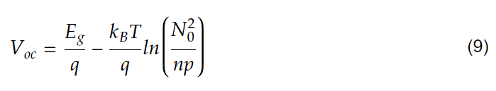
where Eg is the energy of the band-gap, q is the unit charge, kB is the Boltzmann constant, T is the temperature, N0 is the effective density of states, n the electron density and p the hole density.
Open-circuit voltage decay (OCVD)
Open-circuit voltage decay (OCVD, sometimes also called large-signal TPV) measurements reveal information about recombination and shunt resistance. In OCVD measurements, the solar cell is first illuminated by an LED, or a laser, to create charge carriers. Then the light is turned off and the decay of the voltage is measured over time. When the decay of a homogeneous charge carrier density (dn/dt = −β⋅n² with n = p) is inserted into Equation 9 we obtain:

where n(0) is the initial charge carrier density at open-circuit and β is the recombination pre-factor. According to Equation (11), the voltage signal is expected to decay with a logarithmic dependence on time. This is shown in the plots of Figure 8 as grey lines. Parameter β is chosen according to the ‘base’ case. The analytic solution (Equation (11)) does only fit the numerical simulation at the very beginning. The reason is that the charge is not homogeneously distributed inside the device. Close to the electrodes, the densities are higher and charges flow slowly into the middle of the device where they recombine. Zero-dimensional models are therefore not suited to describe the open-circuit voltage decay in p-i-n structured solar cells. The same consideration also applies to recombination coefficients extracted from CELIV using the OTRACE method or to lifetimes determined from TPV or IMVS which are also described in this manuscript.
The OCVD response in perovskite solar cells presents a shoulder at long recording times caused by mobile ions. Recently, Fischer et al. [Fis21] developed a method to determine the concentration and diffusion coefficients of the mobile ions in perovskite solar cells. The method is based on the application of differential capacitance calculation to temperature-dependent OCVD measurements.
Figure 8 shows the OCVD simulation results of the cases defined in Figure 1. All the cases have in common, that the voltage drops significantly beyond 50 ms after light turn-off. This is related to shunt resistance. The most pronounced effect with respect to the ‘base’ case is visible in the case of ‘low shunt resistance’ (Figure 8(d)). Instead of recombining slowly the charges flow through the shunt resistance and deplete the device. When the shunt resistance is decreased the voltage decays more rapidly. The base case has a shunt resistance of 160 MΩ, the kink at 50 ms is caused by this parallel resistance. The voltage decay before 50 ms shows a logarithmic dependence on time. In the case of deep traps, the decay rate is higher as visible in Figure 8(c). With shallow traps, the voltage decay is slower as charges are immobilized when trapped delaying the recombination. In perovskite solar cells, a persistent photovoltage was observed after light turn-off that might be caused by mobile ions [Bau14].

FIGURE 8. OCVD SIMULATIONS FOR ALL CASES IN TABLE 1. THE LIGHT IS TURNED OFF AT T = 0. THE GREY LINE INDICATES THE ANALYTIC SOLUTION (EQUATION (10)) ASSUMING HOMOGENEOUS CHARGE DENSITIES AND PURELY BIMOLECULAR RECOMBINATION.
From OCVD measurements no material parameters can be derived directly. It can, however, be useful for comparing different devices or to perform parameter extraction by fitting numerical simulations (see the last section).
Transient photovoltage and charge carrier lifetime
Transient Photovoltage (small-signal TPV) is frequently performed to estimate the charge carrier lifetimes in organic solar cells. In a TPV experiment, the solar cell is kept at open-circuit voltage under bias illumination. Then an additional small laser pulse (or LED pulse) is applied to the device to create some additional charge that decays exponentially thereafter. If the light pulse is small enough the assumption that the change in density of photogenerated carriers is proportional to the photovoltage increase (Δn ~ ΔV) holds. The voltage decays as:


The concept of ‘charge carrier lifetimes’ stems from the community of silicon solar cells and describes how long on average a minority charge carrier survives in a doped bulk material. A general definition of minority charge carrier lifetime τ is:
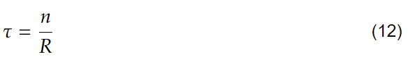
where n is the charge carrier density (electrons or holes) and R is the recombination current. In a device with a high and homogeneous doping density (majority charge carrier), the minority charge carrier has a lifetime that is constant in space and time.
In p-i-n structures, the charge carriers are generated in the intrinsic region and transported to the electron and hole contact layers. The intrinsic region has no doping and consequently also no clear majority or minority carriers. Both electron and hole densities vary spatially even at open-circuit. The charge carrier lifetime is therefore not clearly defined in a p-i-n structure and it is position-dependent. Physical conclusions based on measured ‘charge carrier lifetimes’ can therefore be misleading. Despite these limitations, lifetimes are often determined also for thin p-i-n structured devices. We recommend interpreting measured charge carrier lifetimes from p-i-n structures carefully. In thick devices, the problem is less severe as the charge carrier gradients are smaller.
2.3 Deep-level transient spectroscopy (DLTS)
(Trap Density and Trap Distribution)
Deep-level transient spectroscopy (DLTS) is a technique that was developed to study trapping in semiconductor devices. It can give important information about trap density and trap distribution.
In DLTS a capacitance, a current (i-DLTS), or charge (Q-DLTS) is measured over time after the application of a voltage step at various temperatures. The technique promises to determine trap spectra (trap density versus energetic trap depth) of majority and minority carrier traps as well as capture cross-sections. It is frequently applied to study defect distributions in inorganic semiconductors.

Great care must be taken to accurately determine trap spectra in organic, perovskite, or quantum dots. When measuring capacitance-based DLTS the probing frequency must be small enough to measure the space-charge capacitance. When measuring i-DLTS it is important to properly subtract the displacement current and measure with high current resolution. DLTS has also been performed on perovskite solar cells to determine the trap energies and densities. Such results should, however, be carefully interpreted as the presence of mobile ions may disturb the measurement.
In the following, we analyze i-DLTS. A negative voltage step (from 0 to −5 V) is applied to the device in the dark and the transient current response is analyzed. In addition to the displacement current caused by RC-effects, there is a small current from trap emission. The trap emission current jte from a discrete energy trap can be described as:


We distinguish between two distinct shapes of the current decay from thermal emission of trapped carriers. The emission current from single energy trap levels (Equation (13)) is exponentially decaying. The emission current from an exponential band tail N(E) = ND⋅exp(−E/E0 shows a power-law decay described as:

To illustrate the different current decay shapes, we calculate the emission current from two different densities of states. First, the density of states is filled with charges using Fermi–Dirac-statistics, then the emission current overtime is calculated. Charge transport inside the device is neglected. In Figure 9 the carrier distribution and emission current from an exponential trap-DOS and a Gaussian trap-DOS are shown. The initial Fermi-level was chosen as 0.2 eV. The traps DOS in Figure 9(b) is therefore completely filled. The exponential tail is filled below 0.2 eV. The emission current over time from the exponential DOS follows a power-law decay (Figure 9(c)) and is described well for longer times using Equation (16). The emission from the Gaussian trap DOS is exponential and reflected by Equation (14). In reality, a combination of both may be observed. Furthermore, emission currents from both electrons and holes will make the analysis more difficult. For simplicity, we use single energy traps and discrete band energies for the simulations of DLTS below.

Figure 9. Calculation of the thermal emission of charge carriers from the density of states. (a) The dashed line is the density of states with square-root dependence above the band edge and exponential dependence inside the band. The solid lines represent the charge carrier distributions at different times. The LUMO-level is located at 0 eV, positive energy values reach into the band-gap. (b) Same as in (a) but for a Gaussian DOS. (c) Calculated currents from carrier emission of (a) and (b) including analytical fits according to Equations (14) and (16).
Figure 10 shows DLTS simulations at room temperature. In contrast to the results of the rate equation model in Figure 9(c), the results in Figure 10 were obtained with the drift-diffusion software Setfos which considers the position-dependence of carrier transport in the device. The current peak within the first 1 μs is caused by RC-effects and is not of interest here. The recombination pre-factor and the mobility have no influence on the resulting current (Figure 10(b)). For ‘shallow traps’ an additional current flow from trap emission is observed (Figure 10c)). The deep traps lead to SRH-recombination – trapped charges recombine instead of being re-emitted. An extraction barrier as shown in Figure 10(a) can however lead to a current tail that might be mistaken for trap emission. When the device has a low shunt resistance as shown in Figure 10(d) the trap emission current is hidden by the leakage current through the shunt. If the device is doped some of the equilibrium charges is extracted which leads to an additional current (Figure 10(e)).

Figure 10. DLTS simulations for all cases in Table 1. The voltage is 0 V for t < 0. At t = 0 the voltage jumps to −5 V. (f) DLTS simulations of case ‘shallow traps’ at different temperatures (solid lines). The dashed lines are exponential fits according to Equation (14).
2.4 Transient photocurrent (TPC)
(Trapping and Doping)
In transient photocurrent (TPC) experiments the current response of a photovoltaic device to a light step is measured at constant offset-voltage. The current rise and decay reveal information about the charge carrier mobilities, trapping, and doping. TPC is usually performed with varied offset-voltage, offset-light, or light pulse intensity. The rise time in organic solar cells usually lies between 1 and 100 μs. In perovskite solar cells, the current rise starts in the microsecond regime and can take several seconds until a steady-state is reached.
Polymer solar cells may present a photocurrent overshoot, which can be caused by charge trapping and de-trapping. If the charge trapping is slow enough, it leads to a current overshoot caused by space charge effects. As more and more charges get trapped they screen the electric field and hinder charge transport. Fast trapping however leads to a slower current rise. In some cases, a current overshoot occurs only at negative bias voltage.

The current decay can be described in the same manner as in DLTS (presented before). Using Equation (13) trap emission currents from discrete energies can be calculated. Using Equation (15) trap emission from an exponential DOS tail is calculated.
The extracted charge is obtained by integrating the current decay over time. However, during extraction, most of the charge recombines causing an underestimation of the effective charge inside the device. The magnitude of the underestimation depends on the relative time scale of recombination with respect to charge extraction.
Figure 11 shows TPC response with light pulses of 15 μs duration for the simulated cases presented in Figure 1. The shape of the current rise does not change for the cases: ‘extraction barrier’ (a), ‘non-aligned contact’ (a), ‘high Langevin recombination’ (b), ‘low shunt resistance’ (d), and ‘low charge generation’ (e). A smaller charge carrier mobility clearly leads to a slower rise and decay as shown in Figure 11(b). The shallow traps fill slowly (capture and re-emission) and lead to a slower equilibration of the current (c). The trap emission leads to a slow exponential current decay after light turn-off. The case with deep traps shows a current overshoot (c). Space charge is built up by the charged traps reducing the current on a longer timescale. If TPC is performed with offset light, the current overshoot, and the long decay vanish because the offset light keeps the traps filled. High series resistance can also lead to a slower current rise and decay as shown in Figure 11(d). The case ‘high doping density’ shows a slightly longer current rise and decay caused by space charge effects. With imbalanced mobilities, two-time constants arise corresponding to the fast and the slow carrier type.

Figure 11. Transient photocurrent simulations for all cases in Table 1. At t = 0 the illumination is turned on. At t = 15 μs the illumination is turned off. The applied voltage is 0 V. The current is normalized by the current at 15 μs.
In contrast to CELIV, there is no simple formula to extract the charge carrier mobility from TPC data. TPC is however a powerful technique to study charge transport, identify trapping, and to extract parameters using numerical modeling.
2.5 Charge extraction (CE)
(charge carrier density, transport and recombination)
Charge extraction (CE) was initially introduced to measure the charge carrier density in dye-sensitized solar cells and it is now frequently utilized to measure charge carrier density at varying light intensities. It is sometimes also referred to as photo-induced charge extraction (PICE) or time-resolved charge extraction (TRCE). When a negative extraction voltage is used it is referred to as bias amplified charge extraction (BACE).

In the CE experiment, the solar cell is illuminated and the open-circuit voltage is applied such that no current flows (Voc). In this state, all charge carriers generated by light recombine. At t = 0 the light is switched off and simultaneously the voltage is set to zero (or reverse bias). The charge carriers are extracted by the built-in field and lead to a current. Integrating the extraction current over time yields the extracted charge. The charge carrier density nCE is then calculated according to

where d is the device thickness, q is the unit charge, te is the extraction time (usually 1 ms is enough), j(t) is the transient current density, Cgeom is the geometric capacitance, Va the voltage applied prior extraction (in most cases Voc) and Ve is the extraction voltage. The charge on the capacitance needs to be subtracted because only the charge carrier density inside the bulk is of interest.
When the experiment is performed with varied delay times between light turn-off and charge extraction, CE can also be used to study recombination. The technique is then very similar to CELIV with OTRACE, described in the section above.
Figure 12 shows simulation results of charge extraction for all cases with varied light intensity. Changing the mobility or the recombination pre-factor changes, the open-circuit voltage Voc but has no major influence on the relation charge carrier density versus the Voc (b). The thin grey line is the theoretical open-circuit voltage from a zero dimensional model assuming equal electron and hole densities. At higher light intensity the trend agrees well with the simple model. At low light intensity the zero-dimensional model fails due to stronger spatial separation of electrons and holes.

Figure 12. Charge extraction simulations for varied light intensity (and thus Voc) for all cases defined in Table 1. The current is integrated over time according to Equation (17) to obtain the charge carrier density (the charge on the capacitance is subtracted). The light intensity is varied by five orders of magnitude. The grey-line is the theoretical Voc for n = p in a zero-dimensional model. (f) Extracted charge carrier density at the highest light intensity. Grey lines represent the effective amount of photogenerated charge at open-circuit obtained from the simulated charge carrier profiles.
The case ‘deep traps’ (c) has a similar n vs. Voc curve. The ‘shallow traps’ (c), however, lead to a higher density of extracted charges. Trapped charge carriers are ‘protected’ from recombination. Therefore, a higher charge density can accumulate at Voc. The Voc in the case of‘ non-aligned contact’ (a) is lower. More charge is required to reach the same Voc. It is far away from the ideal curve shown in grey. The series resistance (d) has no influence on the extracted charge. The extraction current is slowed down, but the current-integral remains constant. Interestingly, the charge carrier density is much higher in the case ‘high doping density’. The device is p-doped, so there are less electrons under illumination compared to the un-doped case. Under illumination, the depletion region gets smaller and more holes can accumulate compared to the un-doped case.
In Figure 12(f), the extracted charge at the highest light intensity is compared to the effective photogenerated charge in the device at open-circuit (grey horizontal line). The extracted charge carrier density is in all cases lower, between 15 and 70%, than the effective charge carrier density at open-circuit. Applying a negative extraction voltage Ve reduces recombination losses.
The accuracy of the charge extraction results critically depends on the recombination. Materials with a lower recombination rate or the application of a negative extraction voltage leads to a reduction in recombination losses and a subsequent increase in charge extraction.
References:
3. AC Measurements
The response of the device is measured during the application of an electric or illumination stress in the AC domain, thus it oscillates at a set frequency.
3.1 Impedance spectroscopy (IS)
(traps concentration, trap activation energy, equivalent circuit)
Impedance spectroscopy is a popular technique to investigate solar cells. It is abbreviated as IS or EIS (electrochemical impedance spectroscopy). It is also called admittance spectroscopy (admittance is the inverse of the impedance). The impedance of the device is measured at several frequencies by applying a small sinusoidal voltage and measuring the current in the frequency domain. By using a large range of frequencies different physical effects in the device can be distinguished due to their different transient dynamics. Traps can for example show a larger effect in the low-frequency range.
In IS, a small sinusoidal voltage V(t) is applied to the solar cell according to


Where Iamp is the amplitude current signal and φ is the time delay between V(t) and I(t).
Impedance spectroscopy is performed at various frequencies and/or offset voltages (see next section) and/or offset illuminations. Using the transient voltage and the transient current signal the complex impedance Z is calculated according to:

where Y is the admittance, Zamp=Vamp/Iamp. For the analysis of the impedance, often the capacitance C and the conductance G are plotted versus frequency or offset voltage are calculated according to:
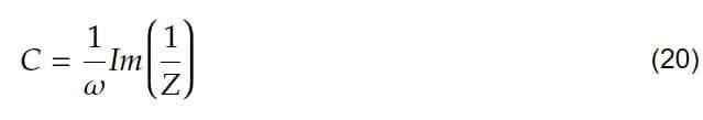

where ω is the angular frequency, Im() denotes the imaginary part, and Re() the real part.
Usually, impedance spectroscopy data is plotted in the so-called Cole-Cole plot. Here, the real and imaginary parts of the impedance Z are plotted in the complex plane for the different frequencies. Alternatively, the capacitance C is plotted versus the frequency.
This technique relies on the depletion approximation, but it cannot be fulfilled in the case of perovskite solar cells due to the presence of mobile ions in the depletion region. Moritz et al. [Mor20] showed that studying the rise and decay of the capacitance allows for distinguishing between capacitance changes due to electronic defect states and mobile ions.
Additionally, Ravishankar et al. [Rav22] demonstrated that the presence of selective contacts with high resistivity influences the capacitance-frequency transitions (step-wise decrease in capacitance). It follows that the apparent activation energy depends on the built-in electrostatic potential drop through the selective contacts.
One of the main advantages of using impedance spectroscopy is that effects occurring on different timescales can be separated. Trapping and de-trapping for example occur usually on a longer time scale (lower frequency) compared to the transport of free carriers. Most commonly, impedance spectroscopy data is analyzed using equivalent circuits. Thereby electric circuits are constructed from resistors, capacitors, inductors, and further electric elements such that the measured frequency-dependent impedance can be reproduced. The disadvantage of equivalent circuits is that the results can be ambiguous and the parameters cannot be directly associated with macroscopic material parameters.
Measuring the capacitance is a way to probe the occupation of trap sites due to space charge effects. Slow traps can increase the capacitance at low frequencies. Also, slow ionic charges which might be present in perovskite solar cells can lead to an increase in the capacitance at low frequencies. Recombination of charge carriers leads to a decrease in the capacitance – it can even become negative. A positive capacitance means that the phase-shift between voltage and current is positive (voltage leading the current), and a negative capacitance means that the phase-shift becomes negative (current leading the voltage).
The real part of the impedance at low frequency coincides with the inverse of the current slope in the JV curve at the same offset voltage. If the probing frequency is low enough one basically measures the DC properties. Thus, a JV curve can be used as a consistency check of the impedance measurement. From low-frequency impedance data, the JV-curve can be reconstructed without using equivalent circuits.
Figure 13 shows the capacitance-frequency profile for all simulated cases presented in Figure 1. In the base case mainly RC effects are observed. Due to the background illumination, the capacitance is however slightly higher than the geometric capacitance of 27 nF/cm². A large amount of charge in the bulk leads to a reduced depletion region – and consequently to a higher capacitance. The extraction barrier (a), the low mobility (b), traps (c), or doping (e), therefore, lead to an increase in the capacitance under illumination. In the case of deep and slow traps (c), this capacitance rise occurs only at a low frequency. If the probing frequency is too high, charges cannot be trapped and de-trapped during one period. These slow traps are therefore invisible at high frequencies (for example 100 kHz in plot Figure 13(c)). With shallow traps the de-trapping is much faster – therefore the capacitance-rise happens already at a faster timescale.

Figure 13. Impedance simulations for all cases in Table 1. The capacitance C is calculated according to Equation (20). The offset-voltage is 0 and offset-light is turned on. The dashed grey line represents the geometric capacitance.

3.2 Capacitance-Voltage (CV)
In capacitance-voltage (CV) measurements the impedance is measured at a constant frequency and the offset-voltage is varied. The capacitance is calculated according to Equation (20). To measure CV usually frequencies below 50 kHz are used. In most diode-like devices, CV shows a peak at forward voltage. The position of this peak is usually independent of the probing frequency and independent of the device thickness. The peak voltage is usually smaller than the built-in voltage and it can be regarded as an effective value for the conduction onset. The height and the voltage of the capacitance peak are related to carrier injection (the injection barriers and the built-in voltage). In bipolar devices like solar cells, the capacitance peak cannot be directly related to an analytical expression.
The increase in the capacitance is caused by a space-charge effect. When the voltage increases charges are injected and the depletion width decreases – leading to an increase in capacitance. After a certain voltage value, the conductivity of the semiconducting layers increases and the capacitance decreases again and can even get negative. Negative capacitances can be caused by recombination or self-heating.
Figure 14 shows CV simulations for all cases presented in Figure 1. Significant changes in the peak voltage are only observed in the cases where the charge injection is changed. The case ‘non-aligned contact’ (a) has a lower built-in voltage which leads to a decrease in the peak voltage. The case ‘extraction barrier’ (a) has the same built-in voltage but an additional barrier to overcome and thus the CV peak is shifted to higher voltages. In all other cases, only a slight change in CV peak voltage is observed. CV seems therefore suited to investigate charge injection and the built-in voltage.

Figure 14. Capacitance-voltage simulations for all cases in Table 1 without offset illumination. The capacitance C is calculated according to Equation (20). The frequency is kept constant at 10 kHz. (f) Voltage where the capacitance reaches a maximum
Mott-Schottky analysis of CV measurements (doping, built-in voltage)
Mott–Schottky analysis is a popular technique applied to CV data to extract the doping density and the built-in voltage using the relation
We propose to include dark-CELIV measurements to estimate the lower limit of the doping density of organic and perovskite solar cells.
The determination of the built-in potential with a Mott–Schottky analysis is also erroneous as shown by Mingebach et al. [Min11]. Mott–Schottky analysis should only be performed on devices that are thick enough and highly doped.

3.3 Intensity-modulated photocurrent spectroscopy (IMPS)
(Charge Transport Lifetime)
In intensity-modulated photocurrent spectroscopy (IMPS) the device is kept at short-circuit conditions while illuminated with a modulated light intensity that varies sinusoidally. The photocurrent is measured. On the contrary, in IS the voltage is modulated, while the light conditions do not vary.
The IMPS experiment can be used to characterize charge carrier transport and obtain information about transport time.
The modulated light intensity L(t) is described as:


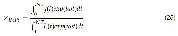
where N is the number of periods, T is the period 1/f, i is the imaginary unit and ω is the angular frequency.

IMPS has also been applied as an imaging technique to study morphological phases in bulk-heterojunction solar cells. In perovskite solar cells, a second peak at 10 Hz was observed and attributed to ionic motion.
Figure 15 shows the imaginary part of the IMPS response for all cases presented in Figure 1. In all cases, a peak at high frequency is observed. It can be related to charge transport – only the case of ‘low mobilities’ (b) leads to a significantly longer transport time-constant and thus the peak shifts to a lower frequency. Trapping and de-trapping (c), as well as an extraction barrier (a), can lead to an additional peak/shoulder at low frequency. The series resistance slows down charge transport (d) as in all transient experiments, thus shifting the peak to a lower frequency. All other cases show no distinct features.
In the case of imbalanced mobilities, two peaks may appear in IMPS measurements.

Figure 15. IMPS simulations for all cases in Table 1 with low offset light intensity (3.6 mW/cm²). The offset voltage is zero. (f) IMPS transport time-constant calculated according to Equation (26).
If you would like to run these measurements with PAIOS, we would be happy to provide a free demo.


3.4 Intensity-modulated photovoltage spectroscopy (IMVS)
In intensity-modulated photovoltage spectroscopy (IMVS), the device is kept at open-circuit so that no current flows while illuminated with a light intensity that varies sinusoidally. The voltage is measured.
IMPS and IMVS are closely related. In IMPS, the voltage is constant and the sinusoidal current is measured. In IMVS the current is zero and the sinusoidal voltage is measured. Classically, from IMVS measurements the charge carrier lifetime is extracted using the frequency where the imaginary part reaches a minimum. As for the transient photovoltage (TPV), the charge carrier lifetime is not quantitatively meaningful in p-i-n structured devices, so it should be considered only for qualitative comparisons.

At open-circuit, the device behavior is not only governed by recombination (as commonly expected), but also by charge transport. Up to now, there is no straightforward interpretation of IMVS measurement results. Charge carrier lifetimes extracted from IMVS and TPV should be fully consistent.
Figure 16 shows the imaginary part of the IMVS response for all cases presented in Figure 1. Figure 16f shows the charge carrier lifetime calculated from the frequency of the IMVS peak. The cases ‘extraction barrier’ and ‘non-aligned contact’ (a) show similar behavior with a peak in the imaginary part. It might seem surprising that the case ‘high Langevin recombination’ (b) has a peak at the same frequency and consequently the same charge carrier lifetime. The reason is that the Voc of the case ‘high Langevin recombination’ is lower at this light intensity.

FIGURE 16. SIMULATION OF IMVS FOR ALL CASES DEFINED IN FIGURE 1. THE OFFSET LIGHT INTENSITY IS 3.6 MW/CM2 AND LIGHT MODULATION AMPLITUDE IS 20% OF THE OFFSET LIGHT INTENSITY. F) IMVS CHARGE CARRIER LIFETIME EXTRACTED FROM THE PEAK FREQUENCY.
References:
4. Further Characterization Techniques
There are a number of other optoelectrical characterization techniques for solar cells that we describe here only briefly without being exhaustive.
4.1 Displacement current measurement (DCM)
Displacement current measurement (DCM) is a technique that is used to study the capacitance of multi-layered devices and estimate trap densities. In DCM, a triangular voltage is applied to the device in the dark in two cycles. Compared to CELIV, in DCM the voltage ramp goes up and down such that both the injection and the extraction of carriers can be studied. When carriers are injected into one layer the capacitance of the multilayer system changes and so does the displacement current. Comparing the first and the second cycle allows one to estimate the trap density.
4.2 Dark injection transients (DIT) and transient SCLC (T-SCLC)
In dark injection transients (DIT), a voltage step is applied to a device and the transient current is measured. The device under investigation needs to be unipolar (only one charge carrier type can be injected) and good Ohmic contacts are required. A space-charge effect leads to a current overshoot. Therefore, this technique is also called transient space-charge-limited current (T-SCLC) in the literature. The time of the current overshoot is related to a transit time and allows the estimation of the charge carrier mobility and its field dependence. The occurrence of the current overshoot is a confirmation of good electrical contact for charge injection.
4.3 Double injection transients
In double injection transients, a voltage step is applied to the device. Compared to dark injection transients this technique is applied to ambipolar devices where electrons and holes can be injected. It leads to a slow current rise until a steady state is reached. The electron mobility, hole mobility, and recombination pre-factor determine the current rise dynamics and can be estimated by formulas.
4.4 Open-circuit voltage versus temperature
In open-circuit voltage versus temperature, the open-circuit voltage is measured at varied temperature to estimate the built-in voltage and the band-gap. We have simulated open-circuit voltages versus temperature and found that the built-in voltage is extracted accurately from Voc at low temperature. With extrapolation to zero Kelvin the band-gap can be extracted accurately except for the cases “non-aligned contact” and “extraction barrier”. The simulation results can be found in the Supplementary Information.
4.5 Differential charging
Differential charging combines small-perturbation transient photocurrent (TPC) and transient photovoltage (TPV) measurements. From the two experiments, the differential capacitance C = ΔQ/ΔV is calculated for varied light intensity. The integral reveals the charge carrier density at open-circuit. The charge ΔQ stems from the current-integral of TPC whereas the ΔV is the change in voltage in TPV. Both experiments are performed with offset-light and a small light pulse.
4.6 Time-delayed collection field (TDCF)
In the time-delayed collection field (TDCF) the device is kept at a constant voltage when a short laser pulse is applied. After a delay-time, a reverse bias is applied to extract the charge carriers. TDCF can be used to investigate the field dependence of charge generation and recombination. A low RC-time is required for this experiment.
4.7 Thermally stimulated current (TSC)
Thermally stimulated current (TSC) is a technique to measure trap spectra in semiconductors. The device is illuminated and cooled to low temperatures (<50 K). Then the illumination is turned off and the device is slowly heated back to room temperature. The current resulting from trap emission is measured over time. Shallow traps are released at low temperatures and deeper traps are released at higher temperatures. Trap density and trap energy levels can be estimated.
4.8 Thermal admittance spectroscopy (TAS)
In thermal admittance spectroscopy (TAS), impedance spectroscopy is measured at different temperature levels. Similar to DLTS, full trap spectra can be extracted by analyzing the capacitance-frequency relation. It is also possible to determine activation energies for mobility and injection.
4.9 Transient absorption spectroscopy (TAS)
Transient absorption spectroscopy (TAS) takes advantage of the fact that in some materials infrared light is absorbed by free-charge carriers. The device is illuminated by infrared light (usually at a wavelength of around 1000 nm) and the transmitted or reflected light is measured with a photo-detector. An additional optical light pulse creates charge carriers that are then monitored over time by the infrared light to investigate recombination dynamics.
4.10 Time-of-flight (TOF)
Time-of-flight (TOF) is a technique to measure the charge carrier mobility in semiconductors. A short laser pulse generates a small number of charge carriers on one side of the semiconductor layer. Due to an applied voltage the charge carrier package drifts through the layer. From the transit time, the mobility is calculated. The advantage of the technique is that electron and hole mobilities can be measured separately. A disadvantage is that the technique requires thick samples (>1 μm) and blocking contacts. Therefore, it cannot easily be applied to regularly prepared solar cells.
FAQ
Which measurements should I start with
Start with JV for baseline performance, then add one transient method and one AC method to reduce ambiguity. The best combination depends on whether your main question is transport, recombination, traps, or ions.
What does impedance spectroscopy measure in perovskite solar cells
It measures the frequency-dependent response of the device and can separate processes by time constant. In perovskites, ionic motion and contact resistivity can dominate low-frequency features, so interpretation needs care.
How do I extract mobility with CELIV
CELIV uses the position and shape of the extraction peak during a voltage ramp to estimate mobility under specific assumptions. RC effects and field redistribution can strongly bias the result, so cross-checks are recommended.
What is the difference between OCVD and TPV
OCVD tracks the voltage decay after a large change in illumination, while TPV measures a small-signal decay on top of a steady operating point. Both are often used to compare recombination dynamics but can be misleading in p-i-n devices if interpreted as a single lifetime number.
Which measurements help diagnose JV hysteresis
Combine scan-rate dependent JV with transient methods and low-frequency AC measurements. Hysteresis that tracks slow time constants is often consistent with ionic effects and interfacial charging.
How can I separate ionic effects from electronic recombination
Look for signatures that move with temperature, frequency, and pre-bias history. Using both transient voltage decay and capacitance or impedance response helps separate slow ionic redistribution from faster electronic processes.
Can I get trap density and trap depth from DLTS in perovskites
DLTS can be informative, but mobile ions and leakage currents can mask or mimic trap emission. Treat extracted spectra as model-dependent unless supported by multiple independent measurements.
What does IMPS tell me
IMPS is commonly used to estimate a transport-related time constant from the frequency response at short circuit. Additional low-frequency features can indicate trapping, barriers, or slow ionic processes.
When is Mott Schottky analysis valid
It can fail in thin-film devices when contacts and low-conductivity layers contribute to the capacitance response. Use it only with thickness and doping constraints in mind and cross-check with other methods.
Can Fluxim recommend a minimal measurement set for my device
Yes. Send your stack, device area, thickness, contacts, and your main question. We will suggest a minimal set and what each measurement can conclude.