Numerical Optimization of Organic and Hybrid Multijunction and Tandem Solar Cells
Introduction
Designing multijunction solar cells requires optimization of a large number of structural and compositional parameters, such as band gaps and layer thicknesses of the component materials, but also the interlayer design for the series connection in the case of the industrially more relevant monolithic tandem devices. Numerical device simulation can provide instrumental insight for the identification of the optimum multilayer configuration. In organic tandems, while the optical simulation of the thin-film layer stacks is routinely used, full optoelectronic device simulation including the recombination junction formed by the interlayer region is not common. In the case of the perovskite-silicon tandem, the widespread use of silicon hetero-junction technologies featuring combinations of large-scale textures with thin-film contact layers, but also the peculiarities of the perovskite materials in terms of the effects of ion-migration pose challenges to both optical and electrical simulation of such multijunction devices.
We address the above challenges using an integrated optoelectronic device simulation framework designed for the numerical optimization of organic solar cell and light-emitting devices. Electrical stimulation of all-organic tandems is enabled by a novel hopping transport model for the description of charge transfer across organic-organic interfaces. The (optical) optimization of fully textured perovskite-silicon tandems, on the other hand, is made possible by combining the models for the light scattering at silicon textures and for the wave propagation in thin-film silicon and perovskite layers into a dedicated multi-scale simulation framework.

Fig. 1. (a) Layer stack and energy level structure of a high-efficiency organic tandem solar cell. (b) SEM image of a hybrid tandem solar cell structure with the perovskite top absorber layer deposited conformally on the both-side textured silicon heterojunction solar cell.
Numerical Simulation Approach
For the simulation of complex tandem solar cell devices, the modeling of transport of charge carriers and excitons needs to be joined with a multi-scale framework for the optical simulation of quasi-1D architectures. For this purpose we make combined use of several modules of Setfos: Optical generation of charge carriers due to light absorption in the active layers is simulated using the absorption module, which in the case of textured interfaces is coupled to the advanced optics module. The multiscale optics approach where a transfer matrix formalism for the optics of coherent layer stacks and a 3D ray-tracing simulation of scattering at large scale textures are coupled to a net-radiation model for incoherent light propagation is shown in Fig. 2(a). The coupling is performed via extraction of transmission and reflection coefficients from the transfer matrix and ray-tracing models to be used in the net-radiation formalism. For the simulation of charge carrier and exciton transport, the drift-diffusion module is used, with generation rates inferred from the optical simulation. The electronic model takes into account the peculiar properties of organic semiconductors in terms of different mobility models reflecting the presence of disorder and localization. For the description of charge transport at hetero-interfaces, which would be suppressed in the drift-diffusion picture, a hopping model in the spirit of the Miller-Abrahams theory of thermally activated tunneling is used [Fig. 2(b)]. Finally, optimization of photovoltaic device performance can be achieved within Setfos either by screening the relevant space of configurational parameters (‘sweep’), or by defining targets for local or global optimization algorithms.

Fig. 2. Models for tandem solar cell simulation: (a) multiscale optics model for conformally coated large-scale textures as in the perovskite-silicon tandem [OptEx]. (b) Miller-Abrahams hopping model for charge transfer at organic-organic hetero-interfaces relevant for tandem OPV [JAP].
Implementation & Results
A. Optimization of organic tandem solar cells
For the simulation of organic tandem solar cells, we consider the high-efficiency device architecture described in Li et al., consisting of a DR3TSBDT:PC71BM top cell and a DPPEZnP- TBO:PC61BM bottom cell, with a recombination interlayer composed of a combination of ZnO nanoparticles and PEDOT:PSS. Thin layers of CuSCN and PFN are used as anode and cathode buffer layers, respectively. The electrodes are formed by ITO and Al. The layer structure and the energy level alignment of the experimental model system used for the simulation are displayed in Fig. 1. Accordingly, HOMO-LUMO levels are taken as indicated in the experimental reference, and the electron and hole transport levels of the individual bulk heterojunctions of the subcells are identified as in Fig. 1(a). The initial layer stack and energy level alignment - including the hetero-interface - are displayed in Fig.3.

Fig. 3. SETFOS implementation of (a) Layer stack with optical and electrical simulation domains as well as (b) energy level alignement including the identification of the hopping interface connecting the subcells.
In order to validate the simulation approach and to extract unknown material parameters for the consistent modeling of single-junction and tandem cells, the experimental JV-curves are fitted using global multi-parameter optimization routines. Starting values for the optical and electrical parameters were taken from the literature. As in the experimental work, the single-junction solar cells were implemented with both absorber materials sandwiched between PEDOT:PSS as HTL and a PFN/Al contact. For the tandem simulation, the single junction material parameter values were taken as starting values and were kept at the same order of magnitude in the optimization of the new parameters for the CuSCN HTL, the ZnO ETL/interlayer, and the attempt-frequency for LUMO-HOMO transfer at the hopping interface. In this way, a good fit of all the JV-curves could be achieved with a consistent parameter set, as displayed in Fig. 4.

Figure 4: Model validation and parameter extraction by consistently fitting the experimental current-voltage characteristics of single-junction and tamdem cells with Setfos, using global optimization algorithms.
Using the material parameters obtained in this way, we then perform structural (i.e., layer thickness) optimization via optical simulation of the layer stack for normally incident illumination under AM1.5g spectrum. The left side of Fig. 5(a) shows the limiting photocurrent as a function of the thickness of top and bottom absorbers as obtained from a “brute force” double sweep over the thickness parameters. The black cross marks the result of the global optimization for the active layer thicknesses with the rest of the layers kept fixed, in perfect agreement with the sweep result for the optimum configuration. In the next step, the number of layers in the global optimization is increased, by subsequently subjecting to the optimization the thicknesses of the CuSCN, the ITO, the ZnO, and the PEDOT layers. The corresponding adjustment of the layer thicknesses is shown on the right side of Fig. 5(a). Starting from the optimum configuration with respect to the optics (grey cross), full opto-electronic device optimization is performed by maximizing the electrical output power of the device. Again, the optimum configuration (black cross) determined via global optimization agrees perfectly with the result of the sweep over active layer thicknesses, while being about one order of magnitude faster to compute. The evolution of the maximum efficiency with an increasing number of layers in the global optimization is displayed in Fig. 5(b) on the right-hand side and demonstrates the potential of the approach to yield device efficiencies significantly exceeding the results obtained by optical optimization only.
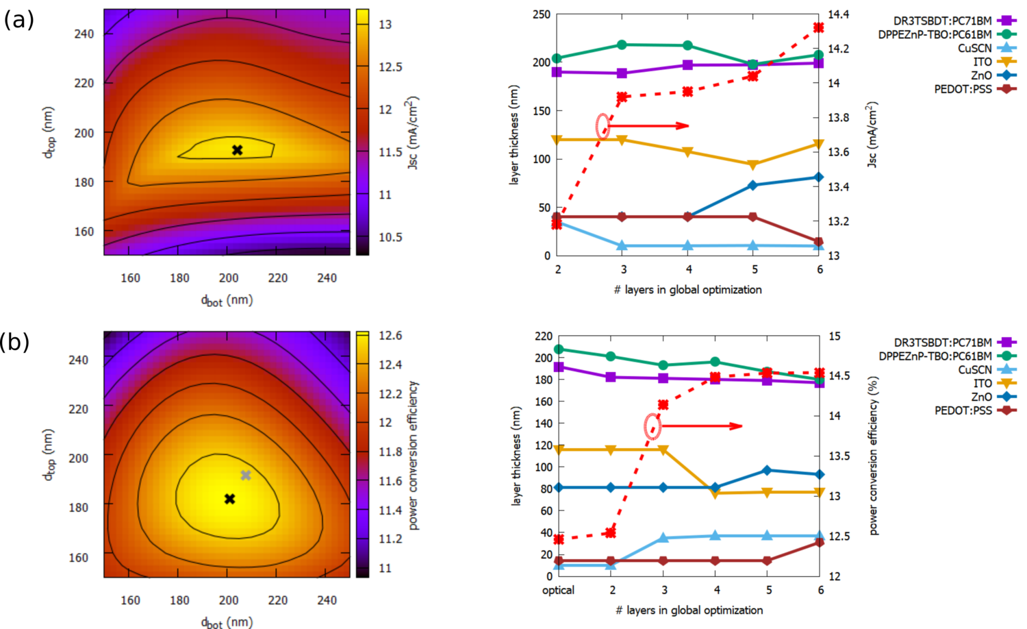
Fig. 5. (a) Left: Optical simulation of limiting photocurrent as a function of the thickness of top and bottom absorbers. The black cross on the ridge of current matching marks the result of the global optimization. Right: Result of optical optimization of the short circuit current density with increasing number of layers, successively adding CuSCN, ITO, ZnO and PEDOT:PSS layer thicknesses to the configurational parameters that are allowed to vary. (b) Left: Coupled opto-electronic simulation of limiting photocurrent as a function of the thickness of top and bottom absorbers. The black cross marks again the result of the global optimization, while the gray cross indicates the solution using the optically optimized configuration. Right: Evolution of the power conversion efficiency upon structural optimization using global optimizer algorithms together with full drift-diffusion device simulations.
B. Optimization of perovskite-silicon tandems
Recently, the above numerical optimization formalism was applied to the optical design of perovskite-silicon tandem solar cells, where the silicon device was a two-side textured silicon heterojunction solar cell, and the perovskite was conformally coated on top of the textured silicon [OptEx]. Successful validation of the optical multi-scale simulation approach was achieved for three different device architectures as displayed in Fig. 6: A – planar cell, B – planar cell with textured anti-reflection foil on the front contact, and C - rear-side textured silicon tandem with a flat interface to the perovskite. For all the devices, a close agreement of simulated with experimental characteristics is achieved.

Fig. 6. Left: Layer stacks used for validation purposes: A – planar structure, B – planar stack with front side texture foil, C – planar top cell and rear-side textured c-Si wafer. Right: Comparison of measured and simulated EQE for a monolithic perovskite-silicon tandem solar cell with the structure as defined on the left.
In a first optimization step, the rear-textured cell with planar top-cell and texture foil at the front contact is simulated for both n-i-p and p-i-n configurations [LHS of Fig. 7 (a) and (b)]. The topography of the texture foil as measured by AFM was directly imported into the simulation. In the optimization procedure, the thicknesses of perovskite and Spiro layers were adjusted in the case of the n-i-p configuration, while in the p-i-n case, only the perovskite layer thickness was varied. The EQE was then fitted via the simulated absorptance under the assumption of an IQE of 95% for the perovskite and 100% for silicon. This yields a strongly increased photocurrent – from 17.0 mA/cm2 to 18.9 mA/cm2 - originating from higher absorptance in both perovskite and silicon layers for the latter configuration [RHS Fig. 7 (a) and (b)], as observed experimentally for a similar structure.

Fig. 7. Left: Device configurations used in the numerical optimization: (a) Rear-side textured c-Si with planar top cell and front side texture foil – n-i-p architecture, (b) same as (a), but for p-i-n architecture, (c) p-i-n configuration on both-side textured c-Si wafer and conformal perovskite layer. Right: Comparison of layer-resolved absorptances for the configurations displayed on the left.
In a further step, the impact of two-side texturing of the silicon c-Si wafer on the photocurrent generation is investigated. For that purpose, the conformal structure displayed in Fig. 7(c) on the left is optimized by adjusting the MgF2 and perovskite layers under full consideration of the conformal textures. As can be inferred from the layer resolved absorptance displayed in Fig. 7(c) on the right, there is an additional gain of photocurrent related to the reduction of reflection losses at long wavelengths, leading to a Jsc of 19.6 mA/cm2. The beneficial effect of the two-sided texture was recently confirmed by the results of an experimental realization of the conformal perovskite deposition approach [Nat. Mater].
In conclusion, we present a comprehensive numerical simulation approach suitable for the design, optimization, and investigation of complex multi-junction device architectures, with important applications in organic and hybrid photovoltaics. The combination of coherent and incoherent optics as well as drift-diffusion with carrier hopping at charge recombination interfaces allows for the simulation-based optimization of state-of-the-art tandem solar cell devices beyond standard estimates by assessing both optical and electronic losses at the proper operating point. This enables the full optoelectronic design of solar cells optimized for realistic working conditions.