characterization and simulation of organic and perovskite lEDs
Organic Light-Emitting Diodes (OLEDs) are the key component of modern displays with high contrast ratio, high level of sharpness, and stunning color gamut. Currently, researchers are also focusing on developing new Light-Emitting Diodes (LEDs), in which perovskites are used as emitting materials. Perovskite LEDs (PeLEDs) are getting more efficient by the day, also thanks to the extensive research on perovskite solar cells. The development of these devices has been possible only through an accurate electrical and optical characterization of both OLEDs and PeLEDs.
Typically, Organic and Perovskite Light Emitting Diodes (LEDs) are characterized only in steady-state to determine and optimize their efficiency. Adding further electro-optical measurement techniques in the frequency and time domain helps to analyze charge carrier and exciton dynamics and provides deeper insights into the physics of the device. In this tutorial, we present first an overview of frequently used measurement techniques and analytical models for OLEDs and perovskite LEDs. A multi-layer OLED with a sky-blue thermally activated delayed fluorescent (TADF) dopant material is employed in this study as a reference device.
The second part of this tutorial focuses on how to systematically fit the measured OLED characteristics with microscopic device simulations, based on a charge drift-diffusion and exciton migration model. Finally, we analyze the correlation and sensitivity of the determined material parameters and use the obtained device model to understand the limitations of the specific OLED device.
The combination of electrical characterizations and full device simulation allows one to determine specific material parameters, such as the charge carrier mobility of all layers.
All these characterizations can be performed with PAIOS. The simulations are carried on with SETFOS.
3. Characterization Techniques for Light Emitting Diodes (LEDs)
3.1. Current-voltage (J-V) and JV-Luminescence (J-V-L) Characteristics
3.2 Impedance Spectroscopy (IS)
3.3. Transient Electroluminescence (TE)
3.6. Double Injection Transient (DIT)
3.7. Displacement Current Measurement (DCM):
3.8. Modulated Electroluminescence Spectroscopy (MELS):
2. Simulation Methods
3. Examples

Introduction
The newest display technologies could not be realized without the developments in organic light-emitting diodes (OLEDs). Despite their commercial success, there are still issues regarding the efficiency and lifetime of these devices to bring the technology to the next level. Similar (or more drastic issues) need to be resolved to develop a LED technology based on perovskite light-emitting materials. It is especially the blue LED that is lagging behind the performance and reliability of the green and red pixels. This affects the overall display operation, pixel layout choice, and performance.1 Therefore, it is important to better understand the device physics, in general, and the origins of degradation in OLEDs. Novel insight into the operating mechanisms will allow for the design and selection of new materials and provide guidance to optimize the device structure.
Besides the traditional solution or film characterization techniques, such as cyclic voltammetry2–4and ultraviolet photoelectron spectroscopy (UPS),5 new materials need to be thoroughly characterized in full multilayer LEDs or specific layer stacks to assess their suitability in real applications. This is also important as material properties may depend on the device fabrication details as well as the specific layer sequence.6–10 Thus, reliable material characterization in organic and perovskite LEDs is a key requirement. Yet, when devices are used as characterization test-beds, the material parameters are still extracted from single measurements on specific samples. This approach is time-consuming, requires high material consumption and the determined parameters are of limited validity because they might depend on the explicit device structure or on the peculiar analytical model that was selected to fit the data.11–13
The preferred way to determine material parameters in organic and perovskite LEDs should be, therefore, to combine numerical simulations with experiments. Often, these comparisons were solely focusing on steady-state analysis.14–16 In such cases, it is necessary to be careful that the analyzed material parameters are unique.17–19 In order to increase the reliability of device simulation, it is inevitable to include complementary measurement techniques in time and/or frequency domain.19–21
In the next section, we are going to present several techniques that are commonly used to characterize organic and perovskite LEDs. If we want to combine different measurement techniques to globally analyse an LED, it is crucial that all measurements are consistent, and that, systematic uncertainties introduced by individual measurement setups for each technique can be excluded. In the present study, this consistency is ensured by using the all-in-one measurement platform Paios which sequentially measures all electrical characteristics of one or several devices without the need to change the contact or the measurement system.23 In this way, any potential degradation between the different measurements can be reduced to a minimum or even completely excluded.3. Characterization Techniques
3.1 Current-Voltage-Luminance
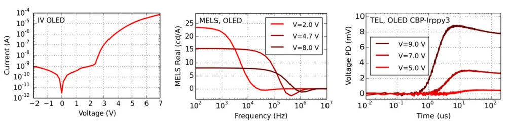
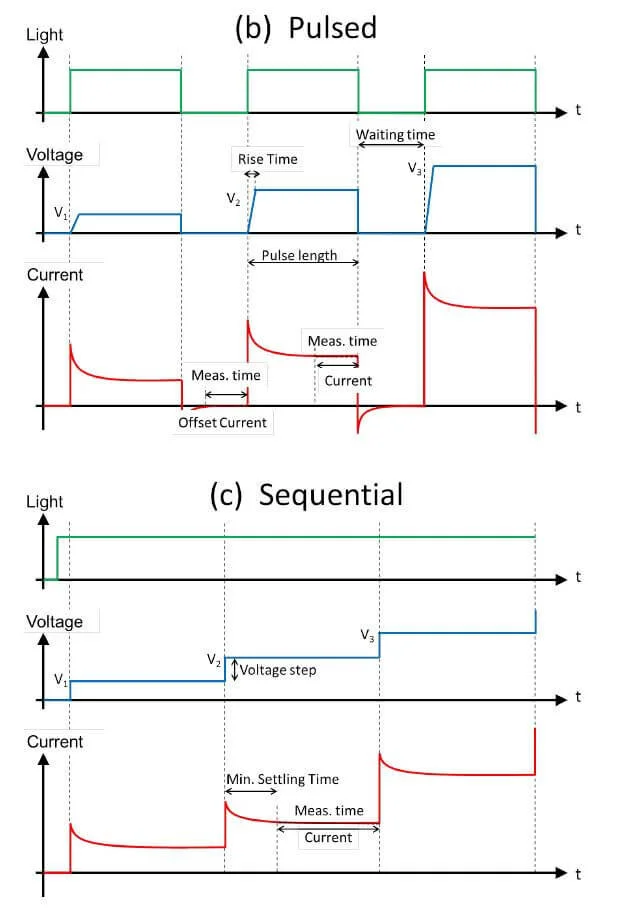
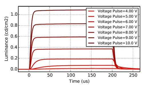
The current-voltage-luminance (IVL) measurement is the basic characterization method for OLEDs and perovskite LEDs. The current-voltage curve is measured as in the normal IV. Additionally the steady-state emission of the OLED is recorded using a photodetector. Knowing the spectrum of the OLED and the sensitivity and geometry of the photodetector the electrical and optical efficiency of the OLED can be calculated. An accurate measurement is performed by using a pulsed voltage, as shown in the Figure. This means that in the best experiment, we are applying a certain voltage Vapp for around 80 ms and subsequently we switch back to 0 V before moving to the next voltage point. The current (luminance) at Vapp is averaged between 20 – 80 ms and the current (luminance) at 0 V is subtracted. Compared to the staircase (sequential) voltage scan, this method ensures reduced self-heating of the OLED and thus allows to go to higher current densities. Moreover, we can compensate for unintentional background light or for electrical noise in the light detection system.
This steady-state characterization is used to quantify the luminous efficiency, current efficacy or external quantum efficiency (EQE). Another interesting parameter which can directly be read from the measurement is the onset voltage (Vonset). In case of sufficient bipolar injection, the onset is usually related to the bandgap of the emitting layer (EML).24 The obtained IV measurement can also be fitted by a single diode model to yield series Rs and parallel resistance Rp as well as reverse saturation current I0 and dark ideality factor n. Parameters that can be extracted from this Analysis: Emission Turn-On Voltage; Working Point; Single Diode Model.


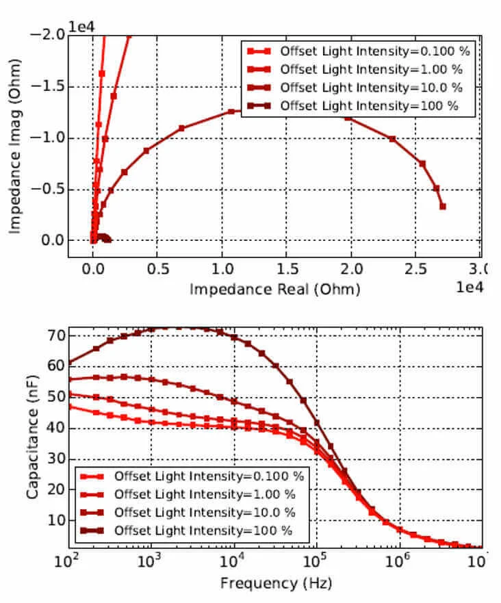
The representation of the IS data can vary. Typically, the conductance G and the capacitance C are evaluated from the real and imaginary part of the admittance, respectively. Either the steady-state voltage V DC is varied at a fixed frequency f or the frequency is varied at a constant V DC . Here we evaluate capacitance- (C-f) and conductance-frequency (G-f) plots at different V DC . The amplitude of the oscillating voltage was always 70 mV. The benefit of considering the capacitance is that for interpretation of the data it can be related to the geometrical capacitance of the device and to parallel-plate capacitances of individual layers or set of layers. Another popular representation is the use of real and imaginary parts of the impedance Z. Moreover, the capacitive response can for instance be used to determine the relative permittivity of the organic materials, assuming the OLED to be well represented by a parallel plate capacitor. In specific cases there are analytical formulas that can be used to determine the charge carrier mobility. 19,31 Qualitatively, impedance data can also be used to investigate charge carrier injection, accumulation and trap states. 17,19,21,25,26,29–33 Often, the impedance measurements are fitted by equivalent circuits. 28,29,34,35 In order to gain some knowledge on the operation principle of the investigated device, the individual elements of the electrical circuit have to be assigned to different layers and physical processes. Depending on the complexity of the chosen equivalent circuit this assignment can be ambiguous. Reliable material parameter extraction is therefore challenging.
If you want to understand how to perform these measurements with PAIOS, just let us known
3.3 Transient Electroluminescence
For a transient electroluminescence (TEL) measurement, a rectangular voltage pulse V is applied to the OLED with varied amplitude. The length of the pulse is chosen such that steady-state conditions are reached at the end of the pulse. Both, the rise of the luminance signal as well as the decay can provide valuable insight into charge carrier and exciton dynamics in the OLED.
The measured characteristic onset time in the TEL signal can be related to the transit time t tr , i.e. the time it takes for the charge carriers to be injected and transported before meeting and recombining radiatively. Thus, the onset time directly reflects the two charge carrier mobilities of electrons and holes. An analytical relation between the transit time ttr and the charge carrier mobility µ is given by 36

where d is the thickness of the device and Vbi the built-in potential. Usually the transit time is approximated by the delay time td between the voltage turn-on and the light onset which might lead to an overestimation of the mobility. 36 This simple formula was developed for single-layer devices which are not injection limited and neglects the spatial variation of the electric field due to the accumulated charge. 36–38 In multi-layer bipolar devices, the relevant thickness parameter d corresponds to the distance which the slower charge carrier needs to travel in order to meet and recombine with the counter-charge. Even though in state-of-the-art OLEDs the onset analysis only yields an apparent mobility, the technique can nevertheless be very useful to qualitatively understand basic charge transport phenomena. 39 The analysis of the TEL rise dynamics is not discussed here in detail for sake of brevity, even though fast and subsequent slow rise can be assigned to the two carriers in the emission layer36 and sometimes a TEL onset overshoot can be observed due to rapid depletion of internally accumulated charges. 40
The TEL decay, however, is generally related to exciton dynamics and interpreted similarly to transient photoluminescence (TRPL). A single exponential decay fit yields an exciton lifetime that can be related to the radiative and non-radiative recombination rates. In contrast to TRPL also charge carriers are present in a TEL experiment. Therefore the decay can be affected by exciton-polaron interactions41 and delayed recombination of charge carriers. 20 Such TEL data have been analyzed in depth do understand different losses in OLED devices 20,42,43 as well as changes during device degradation. 44 Parameter that can be extracted from a TE analyis: Luminescence Lifetime; Field Dependent Charge Carrier Mobility.
3.4 Injection CELIV
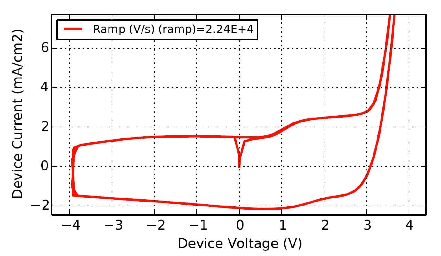
Charge extraction by linearly increasing voltage (CELIV) has first been presented as an analysis technique for inorganic solar cell devices. 45,46 In this experiment, mobile charge carriers that are present in the device are extracted by a reverse voltage ramp (triangular pulse). The associated current is composed of a constant displacement current and an overshoot which is related to the extracted charge carriers. Depending on the way that charge carriers are generated inside the device, one can distinguish between dark- (doping), photo- (light pulse) and injection-CELIV (offset voltage). While the second is commonly used for organic solar cells 11,13,26,47,48 the last is mostly employed in metal-insulator-semiconductor (MIS) devices as well as in OLEDs. 30,49,50 It is also suitable for the analyis of perovskite LEDs.

In all CELIV techniques, the characteristic current peak area, namely the time integral of the current overshoot, can be analyzed to estimate the amount of accumulated charge in the device. The peak time t max is related to the charge carrier mobility µ following the analytically derived formula

where d is the thickness of the device and A is the employed voltage ramp. Several modifications of this formula have been presented to account for commonly neglected effects such as the non-uniform field and charge distribution, series resistance and recombination. 51–56 As for the TEL rise, the use of multilayer OLED structures complicates or even excludes the application of the analytical formula to extract charge carrier mobilities accurately and assign the mobility value to a specific material or carrier type. In such devices the technique should rather be used as qualitative assessment of charge carrier dynamics, e.g.to analyze differences between devices or to identify systematic changes upon degradation.
3.5 Dark CELIV

In the dark-CELIV a negative voltage ramp is applied to the device in the dark. From the initial current rise and the later constant displacement current the series resistance and the geometric capacitance can be evaluated. In case intrinsic charge carriers are extracted they lead to a current overshoot, whose peak time is related to the charge carrier mobility. By integrating the current overshoot the doping density can be estimated.
Parameters that can be extracted from a dark-CELIV analysis:
Doping density, Relative permittivity, Series resistance, charge carrier mobility
3.6 Dark and Double Injection Transient (DIT)

The dark injection transient current is a technique to determine the mobility in thick unipolar layers. A voltage pulse is applied to the device and its current is recorded. The injection current is superimposed with the displacement current due to the voltage step. In the unipolar and trap-free case, a current peak can occur whose position is related to the charge carrier mobility. From the transient position of the peak the charge carrier mobility can be determined by using:

The technique can also be performed in bipolar devices as double injection transient. Here a peak can occur as well, and the dynamics of the rise of the injection current can be analysed. There is, however, no analytic model for this case, and the measurement needs to be compared to simulation.
Parameters that can be extracted from a DIT analysis:
Charge carrier mobility
3.7 Displacement Current Measurement (DCM):
This technique applies a double zigzag voltage ramp to the device, basically repeating a CELIV forward and reverse ramp. The forward voltage ramp probes charge injection, while the reverse ramp probes extraction, being basically a very slow injection-CELIV measurement. The ramp always induces a constant displacement current in the device, on top of which other effects may be observed. At slow ramps there should be a coincidence with the capacitance-voltage shape.
In OLEDs the technique has been used to quantify the trap density and the dipole sheet density in polar materials.
Parameters that can be extracted from a DCM analysis:
Geometric Capacitance, Relative Permittivities and Trap Density
3.8 Modulated Electroluminescence Spectroscopy (MELS):

During a MELS experiment, on top of the operating voltage a sinusoidal voltage is applied to the OLED. Instead of the current as in impedance, the sinusoidal response of the light emission is measured with a photodetector and analyzed. With MELS is possible to gain insights on how sub-bandgap defect states effects the minority carrier recombination dynamic.
Parameters that can be extracted from a MELS analysis:
Effect of Trap States on the LED characteristics.
All these measurements can be performed with PAIOS. We will be glad to discuss with you
B - Sample Design
The OLED structure that has been employed for this case-study is shown in the Figure. The layer sequence and the sky-blue emitter is similar to the one described by Peng et al.22 and represents a prototypical OLED structure that is frequently used in academic and industrial research. The well-known materials NPB (N,N′-di(1-naphthyl)-N,N′-diphenyl-(1,1′-biphenyl)-4,4′-diamine) and TCTA (tris(4-(9H-carbazol-9-yl)phenyl)amine) are used as hole transport and exciton blocking material, respectively. The emitter exhibits thermally activated delayed fluorescent (TADF) properties and is blended into the mCBP (3,3′-di(9H-carbazol-9-yl)-1,1′-biphenyl) host with a concentration of 20 vol.-%. Here, we investigate a systematic thickness variation of the hole transport layer NPB as well as of the electron transport layer NBPhen (2,9-di(naphthalen-2-yl)-4,7-diphenyl-1,10-phenanthroline) layer. Among others, this variation allows us to determine the relative permittivity of the NPB and the NBPhen layer directly from the measured device capacitance (see section III. A.).

Because for state-of-the-art multilayer OLED stacks the above presented analytical formulas are only of limited validity to determine material parameters, full device modelling should be used preferably. The electrical simulations applied in the present study are based on the drift-diffusion approach which has been presented in many previous publications. 17,31,38
The equations can be solved in steady-state, transient and frequency domain to reproduce the measured curves of the electrical experiments. For electro-optical simulations the calculated exciton densities are transferred to the optical solver which is based on the dipole emission and transfer matrix models. 57,58 The commercially available simulation software Setfos is used in this study. 59
The required inputs for the simulation are the layer sequence with respective thicknesses, the refractive indices, and the electrical and excitonic material parameters of each layer. Here, for simplification, and motivated by the band diagram in Figure 1(a), we choose discrete energy levels for transport and traps. For the emitter layer, charge transport is assumed to occur on the mCBP HOMO (holes) and the LUMO of the emitter (electrons). In this example the OLED stack consist mostly of standard materials without any electrical doping.
We set up a protocol, which is shown as flow chart in Figure 2(a). This procedure shall be employed to simulate the measured data on the OLED devices presented in Figure 1.
A full electrical characterization of an OLED typically consists of various steady-state, transient and impedance measurements. As a first step, a selection of relevant results has to be performed. In general, it is recommended to consider as many experimental techniques as possible. One should thus try to select measurements that yield complementary data, but avoid to include multiple similar experiments that contain the same information. For instance, injection-CELIV data at one or two different offset voltages is usually enough. In a second step, we determine those device and material parameters that can be extracted from simple post-processing techniques (e.g. series resistance). Next, the initial guess simulation is set up using measured, assumed, or literature values for the missing material parameters. Importantly, in order to minimize the number of free parameters, and in agreement with Occam’s razor, the initial model should be as simple as possible. Applied to the present case study, this means for example that we shall neglect any trap states at first, and only introduce them in case the simple model fails to properly describe the measured data. After a first simulation of the initial situation one should vary all fitting parameters to learn about their effect on the different measurement techniques. This also allows to manually optimize these parameters in a next step in order to match the experimental data as well as possible. If the agreement after the optimization is not sufficient, new model parameters should be introduced, for example trap states, and the optimization should be done again. Finally, once the agreement between simulation and measurements is satisfying, the fit quality should be analyzed. This task consists of a parameter correlation 17,18 and sensitivity 19,60 analysis.

Figure 2. (a) Workflow to obtain a global fit for various measurement techniques, and to analyze the quality of the resulting fit.
Examples
We will guide the reader through the workflow illustrated in Figure 2 on the basis of real measurements on OLEDs. The selected experimental data which we want to reproduce with device simulations is shown in Figure 3.
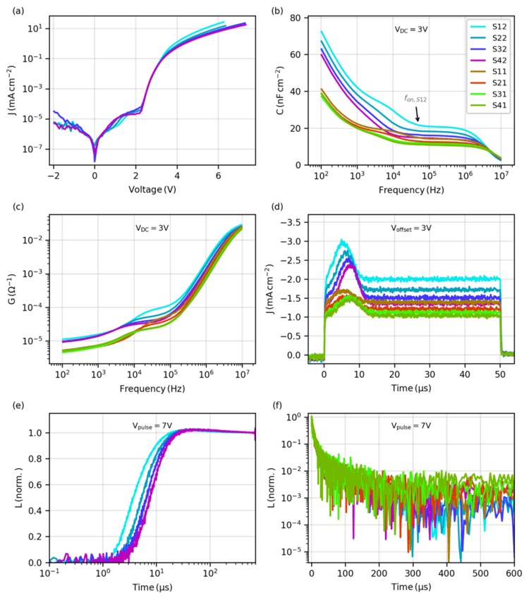
Figure 3. Selected experimental data sets that will serve as a target in the fitting process. (a) Current-voltage, (b) capacitance-frequency at VDC = 3 V, (c) conductance-frequency at VDC = 3 V, (d) injection-CELIV at Voffset = 3 V, transient electroluminescence rise (e) and decay (f) for a voltage pulse of 7 V. In (a) and (e) not all measured 8 devices are shown for the sake of visibility (see supporting material Figure S1I for complete data).
Simulation can also help you speeding up your experimental work. You can evaluate Setfos for free
The IV curve shows an onset at about 2.2 V for all devices with 40 nm thick NPB. As this parameter is mostly determined by the built-in potential it could be speculated that the effect is caused by the fabrication process. Furthermore, the current in the on state (above 3 V) is systematically reduced with increasing NPB thickness. This indicates that the current at high voltages is limited by hole transport inside the NPB layer.
The capacitance and conductance at V DC = 3 V are shown in Figure 3 (b) and (c), respectively. In the frequency range between 10 5 – 10 6 Hz the capacitance reflects the geometrical capacitance of the full device which is also determined at V DC = 0 V. Towards lower frequencies, a capacitance rise is observed which is related to injection of charge carriers. This characteristic frequency f on (see Figure 3b) is independent of the NBPhen layer thickness but shows a dependence on NPB thickness, indicating that the onset is related to hole injection and transport. A second rise is observed at a frequency around 1 kHz for all devices and needs to be linked to a process with slower dynamics.
The conductance between 10 4 – 10 5 Hz shows a similar thickness dependence as the IV characteristics at higher voltages. Towards lower frequencies it converges to one conductance value for all devices that have the same NBPhen thickness which is in agreement with the current in the IV measurement at the same voltage (3 V). We attribute this behavior to charge carriers (holes) that are already present in the device at 3 V and accumulate either at the TCTA/EML or at the EML/NBPhen interface. The remaining NBPhen (and EML) layer(s) is (are) thus limiting the conductivity at this voltage.
Injection-CELIV was performed at several offset voltages. For discussion and simulation purposes we chose an offset voltage of 3 V which is just above the turn-on voltage of the OLED. At this low offset voltage only small amounts of charges are injected that accumulate at some internal interface and are then extracted by the reverse voltage ramp. As outlined in section II, the peak time is related to the charge carrier mobility. For devices with the same NPB but different NBPhen thickness, the peak occurs at the same time (Figure 3(b)). Only the peak area changes which can be explained by the different amount of charge that was injected. The NPB thickness variation results in a clear peak shift. Judging from the observed independence of t max from the electron transport layer thickness, we can already attribute the peak to an effective hole transport time. However, without knowing the interface at which charges accumulate prior to the CELIV ramp we cannot estimate a reliable value for the hole mobility. Additionally, for multilayer structures one can only obtain an average hole mobility which is not directly related to one specific layer. It is worth noting that the measured displacement current plateau value for times t > 15 μs is in perfect agreement with the geometric capacitance of the devices measured by impedance spectroscopy.
The TEL rise and decay for a voltage pulse of 7 V are shown in Figure 3 (e) and (f), respectively. The TEL turn-on time is related to charge transport and injection and shows a similar NPB thickness dependence as the IV curve, the first C-f onset and the injection-CELIV peak time. As for the injection-CELIV peak we cannot directly extract a mobility using the analytical formula. However, from the thickness trend we can see that the TEL onset is limited by hole transport to the emission zone. This qualitative understanding can already provide first insight in view of OLED device design and optimization. In addition to the onset time trends, a small luminance overshoot is observed for all devices before they reach their steady-state luminance at the end of the pulse. Below we will illustrate that this behavior can be related to a trapping effect in one of the hole transport layers.
In the TEL decay we do not see any difference among the devices of varying thickness. By fitting a single exponential decay to the first decay we can extract a radiative lifetime of about 5 us. This agrees well with the delayed fluorescence lifetime of the investigated TADF emitter measured by transient photoluminescence (PL) of the pure emitter film (data not shown). Interestingly, the modified cavity defined by the different layer thicknesses does not influence this decay lifetime. This finding might be related to the TADF emitter for which the reverse intersystem crossing is dominating the decay dynamics.
The above qualitative discussion demonstrates how much more information can be obtained for a specific OLED stack if consistent data with varied layer thickness is available. When fitting the experimental data in the following, the value of the complementary data set becomes even more evident.
As indicated in Figure 2(a) some device and material parameters can directly be extracted from the measurements and should be determined before setting up the simulation. The first parameters are the external series resistance Rs and parallel resistance Rp of the cells. As they depend on the contact quality as well as some shunts that may occur for one or the other cell, these parameters are extracted for each cell and not considered as global parameters. Nevertheless, it turns out that these values are very similar for all the tested devices reported here. R s is determined by fitting the C-f measurement at V DC = 0 V with an equivalent circuit model (Rs+[Rp||C]). A single diode model was adapted to the IV curve to give Rp. 17
Further parameters that can be determined directly from the measurement data are the relative permittivities e of the individual organic layers. First, one has to ensure that the C-f plateau at V DC = 0 V corresponds to the geometrical capacitance of all the semiconducting layers. This was checked by multiplying the capacitance with the total thickness. All devices with varied NPB and NBPhen layer thicknesses give almost the same value which indicates that we are probing the full device. Especially if highly doped or intrinsically polar layers are included, this condition is not necessarily fulfilled and the extraction of the relative permittivity is more difficult.19,21 Here, the geometrical capacitance of the total device is determined from the C-f plateau at V DC = 0 V. Assuming a parallel plate capacitor for each layer, the total capacitance is given by a serial connection of each layer’s capacitance. Thanks to the variation of the NPB (NBPhen) thickness we can directly plot C-1 vs. d NPB (dNBPhen), which is supposed to be linear with a slope corresponding to the permittivity of NPB (NBPhen). The permittivity of TCTA and the EML cannot be independently extracted as there is no thickness variation of these layers.
In order to perform a full electro-optical simulation we also need refractive indices of all the layers. Most of them are available from the Setfos database or were taken from literature. 59,61,62 For the EML spectroscopic ellipsometry was performed on a film. Furthermore, the emitter source spectrum was measured by PL on a pure emitter film. The HOMO and LUMO energies were taken from literature. 16,20,22,63–65 Due to the uncertainty in the determination of the LUMO, 66,67 this parameter was allowed to be changed by up to 0.5 eV during the fitting. The remaining electrical parameters, i.e. hole and electron injection barriers, density of chargeable sites, hole and electron mobilities for each of the layers were guessed or taken from literature if available. 68–71 Here, the respective mobilities are described by the field-dependent Poole-Frenkel mobility model,

where μ 0 is the zero-field mobility and γ the field-enhancement factor.By the choice of this mobility model, with only two free parameters, we follow the principle of Occam’s razor. This parametrization of charge mobility does not include any direct charge carrier dependence. If temperature-dependent measurements would be simulated, both charge- and field-dependence could be considered more easily by using the extended Gaussian/correlated disorder model (EGDM/ECDM). 72,73 While the solution of the EGDM/ECDM has been presented before in steady-state, the implementation to solve multilayer structures in time and frequency domain is much more challenging. As the inclusion of transient and impedance data plays a key role in this analysis we choose the Poole-Frenkel mobility model which is the simplest model at room temperature that can well describe the presented experimental data.
Whenever more complicated device structures, doped layers or new transport materials are investigated, it is generally useful to first measure and simulate elementary devices, such as single-carrier devices, and then gradually increase the complexity of the investigated stack. 15 It has to be noted here, that the choice for the mobility values of the minority carriers, i.e. the electron (hole) mobilities in the NPB and TCTA (NBPhen), has a negligible effect on the simulated curves. Therefore, they are not used as fitting parameters in the following. To couple the electrical characteristics with the optical measurements, excitonic parameters have to be known. For our TADF system, radiative, non-radiative and intersystem crossing rates were extracted from a transient PL experiment with an emitter film sample. These parameters were used as input for the initial guess simulation. The full list of parameters used and obtain during our analysis can be found in our JAP publication (https://aip.scitation.org/doi/full/10.1063/1.5132599).
For the first simulations (initial guess), the assumed model is as simple as possible, i.e. no trap states are included in any of the layers. Starting from this model using the above initial parameters we can now perform the simulations for each of the measurement techniques and device configurations (see Figure 4).
The initial forward simulation is well capable of reproducing some trends, e.g. the HTL thickness dependence in the IV. Nevertheless, several important experimental observations are not yet well captured by the simulations. An obvious example is the TEL rise which occurs about one order of magnitude too late in the simulation compared to the experiment. Thanks to the trends with varied NPB and NBPhen layer thickness, we can already conclude that we need to adjust the hole mobility in one of the hole transport layers or the EML, or the hole (injection) barriers between the layers.
In the next section we will systematically assess the influence of the parameters on the simulated curves, and adapt them to obtain a quantitative agreement with the measured characteristics.

Figure 4. Measured data (solid line) and simulation using initial parameters : (a) Current-voltage, (b) capacitance-frequency at VDC = 3 V, (c) conductance-frequency at VDC = 3 V, (d) injection-CELIV at Voffset = 3 V, transient electroluminescence rise (e) and decay (f) for a voltage pulse of 7 V. For better visibility only selected devices are shown.
First, we notice that the simulated IV onset voltage (Vonset) is not in agreement with the measurements. The only parameter which influences this voltage is the built-in potential. In order to match the measured onset, we therefore decrease all LUMO levels by 0.15 eV in energy while keeping the energy barriers the same. After this adaption, the energy levels are now fixed for all the following optimization steps.
As mentioned above, thanks to the thickness dependence we already know that some hole mobilities have to be increased in the simulation to improve the agreement with the measurement in TEL rise and injection-CELIV. However, we cannot easily distinguish between the hole mobility in NPB, TCTA or in the EML. In order to quantitatively understand which parameter is influencing the electrical device characteristics in which way, we perform individual parameter sweeps starting from the initial simulation shown in Figure 4. As examples we show the influence of the NPB, TCTA, EML zero-field hole mobilities, the field-enhancement coefficient for NPB as well as the zero-field electron mobilities in the EML and the NBPhen on the IV (Figure 5), the TEL rise, the injection-CELIV signal and the C-f plot (Figures S4 – S6). In order to simplify the graph, we only show the parameter variation for device S42.

Figure 5. Influence of the material parameters (a) NPB, (b) TCTA, (c) EML zero-field hole mobility, (d) NPB mobility field-enhancement factor, (e) EML and (f) NBPhen zero-field electron mobility on the simulated IV curve. The dashed grey line represents the measurement on device S42.
The largest influence on the IV curve is observed for the zero-field hole mobility and the field-enhancement factor of the NPB. While the former gradually increases the forward current, the latter also influences the power law of the current above 2.5 V. Thus, we will clearly need to increase the latter in order to fit the experimental data. Interestingly, the charge carrier mobilities in the EML mostly affect the region just after Vonset. Especially the electron mobility should be decreased to match the slope of the IV between 2 – 3 V. The TCTA hole mobility and the NBPhen electron mobility have only a minor effect on the simulated IV curve. Using only these 6 parameters would allow to obtain a decent fit of the IV curve. However, we also want to include the impedance and transient signals in order to increase the reliability of the extracted parameters. This is illustrated by the cases of the hole and electron mobilities in the EML which affect the IV only slightly. While the EML hole mobility clearly shifts the TEL onset, the electron mobility has no effect on the onset time (Figure S6). In the case of injection-CELIV, both mobilities have an influence on the peak position tmax: increasing or decreasing the EML hole or electron mobility shifts the peak position to shorter or longer times, respectively. This example highlights the importance of combining several measurement techniques, as the unknown parameters are reflected differently in each experiment.
As a next step, we will adjust the parameters to match the simulation with the selected key measurements. This can either be done with an automatic optimization/fitting algorithm or by manual tweaking of single parameters according to the observations in the parameter sweeps (Figure 5 and Figures S4 – S6). Automatic least-square fitting algorithms, such as Levenberg-Marquardt or simulated annealing, try to minimize the error χ between the measurement m and the simulation s for N user-defined target points which can be weighted by a factor w.

Due to the multiple devices and measurement techniques which should be optimized together, the selection of the target points and individual weighting factors wi is not straightforward. The optimization is therefore done manually in this example. Furthermore, the fit quality is not evaluated quantitatively by an absolute error but judged by eye. The best fit that was obtained for the current model (no traps included) is shown in Figure 6.
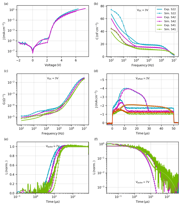
Figure 6. First fit of the selected measurements without considering any trap states. The simulations are shown as solid lines with open circles. (a) Current-voltage, (b) capacitance-frequency at VDC = 3 V, (c) conductance-frequency at VDC = 3 V, (d) injection-CELIV at Voffset = 3 V, transient electroluminescence rise (e) and decay (f) for a voltage pulse of 7 V. For better visibility only selected devices are shown.
This first fit is already able to reproduce the IV curve above turn-on very well. Also, the trends with varied NPB and NBPhen layer thickness in the TEL and injection-CELIV curves are well reproduced. However, the injection-CELIV peak is clearly too large which indicates that too many charge carriers are accumulated and extracted in the modeled device. The simulated impedance data shows quantitatively the same result as the measured C-f and G-f characteristics at 3 V. The NBPhen thickness dependence is however not correctly reproduced. Finally, also the fit of TEL decay (Figure 6(f)) still needs some fine tuning of the parameters. This measurement is the only one which is dominated by excitonic parameters, i.e. Krad,s, Knr,T, kisc and Krisc. These parameters can therefore be independently adapted to match the TEL decay signal. The resulting simulated TEL decay curve is shown in Figure 8(f).
The other electro-optical simulations cannot be adapted further to improve the agreement with the experimental data using the existing model that does not consider any trap states. Therefore, according to the workflow in Figure 2, we shall diversify the model and include additional material parameters. The main features that we want to reproduce in a better way with the simulations are (1) the injection-CELIV peak area which is currently too large in the simulation, as well as (2) the NBPhen thickness dependence in the C-f and G-f data. As mentioned before, the injection-CELIV transient at Voffset = 3 V is mainly determined by hole transport parameters. We therefore first analyze the effect of including hole traps in the NPB, TCTA and the EML layer. We find that including hole traps in the EML does not affect the injection-CELIV peak at all. Therefore we do not further consider any hole traps in this layer. In striking contrast, for the NPB and TCTA layers, the hole trap density as well as the trap energy in TCTA have a significant impact on the CELIV peak area. The corresponding simulations of the injection-CELIV and the IV curve are shown in Figure 7. In more detail, we see that both the TCTA hole trap density and the trap depth have a very similar influence on the CELIV transient and to some extent also on the IV curve. This indicates that the parameters “trap density pt” and “trap depth ΔEt,p” are correlated, which will also be discussed and quantified in Section III. D. Furthermore, we see from Figure 7 that including as many TCTA traps as necessary to match the injection-CELIV peak area will clearly deteriorate the IV behavior. We will therefore also need to include some traps in the NPB layer.
The effect of the NPB trap density is shown in Figure 7(c,f). As for the TCTA layer, the traps’ depth has a very similar effect on the simulated curves as their density (see Figure S7). In contrast to the traps in the TCTA layer, which mainly shift the CELIV peak in time while the qualitative shape is maintained, the traps in the NPB also change the shape of the injection-CELIV peak. In some cases, even a double peak is observed. In order to find a good fit for both the IV and the injection-CELIV data we need to include and optimize the trap parameters in both the NPB and the TCTA layer. As an additional positive effect, the inclusion of hole traps in TCTA and NPB leads to a small TEL overshoot in the simulation which was also confirmed experimentally. Without trap states, the simulated TEL signal never exhibits an overshoot. The overshoot height can be adjusted by the capture rate of hole traps in the TCTA and NPB layer.

Figure 7. Influence of the trap parameters in the TCTA (a,b,d,e) and NPB layer (c,f) on the simulated injection-CELIV (a-c) and IV curve (d-f). The dashed grey line represents the measurement on device S42.
In order to reproduce the measured NBPhen thickness dependence in the IS data, it is required to introduce electron traps in this layer. As shown in Figure 6 (b) and (c), the simulated capacitance and conductance of samples S41 and S42 converge to the same low frequency value, while a clear thickness dependence is observed in the measurement. Gradually increasing the trap density or the trap depth will increase the distance between the simulated curves of device S41 and S42. Again, this demonstrates the importance of having several devices with varied layer thicknesses. It would not have been possible to identify the presence of trap states in the NBPhen if there would have been only devices with one layer thicknesses.
After optimizing the trap parameters together with the other electronic material parameters, we obtain the final fit shown in Figure 8. We can see that all the main features in the measurements are well captured for all the devices. Remarkably, the global fit covers 8 devices with different NPB and NBPhen layer thickness combinations using a single same set of material parameters.

Figure 8. Final fit of the selected measurements considering traps in the NPB, TCTA and NBPhen layer. The simulations are shown as solid line with open circles. (a) Current-voltage, (b) capacitance-frequency at VDC = 3 V, (c) conductance-frequency at VDC = 3 V, (d) injection-CELIV at Voffset = 3 V, transient electroluminescence rise (e) and decay (f) for a voltage pulse of 7 V. For better visibility only selected devices are shown.
Before the reliability of the extracted material parameters is analyzed in the next section, we show how the simulation can further be used to understand device performance and analyze possible loss mechanisms. First, it is possible to analyze electrical profiles of the device at any working point. As an example, Figure 9 shows the recombination profile of the S42 device as a function of voltage. The recombination between 2 – 3 V is almost constant in the full EML. With higher voltages the recombination zone gets narrower and settles at the EML/NBPhen interface. This is in agreement with previous findings by Peng et al., who reported an exponentially decaying emission zone at the ETL interface with a width of about 7 nm using a very similar OLED structure.22 Such an accumulation of charge carriers at one interface of the EML is not ideal because degradation of organic molecules will predominantly occur at locations of high charge carrier and exciton concentrations.22,74,75 A broadening of the emission zone is therefore desirable to increase the stability of this OLED structure. In this example, the electron transport in the EML host-guest layer is assumed to occur on the emitter molecules themselves. Because the emitter concentration is low (20%) the electron transport is limited, which is also reflected in the extracted mobility parameters for the EML. The zero-field electron mobility is about seven orders of magnitude smaller than the zero-field hole mobility of the EML. Balancing the EML mobilities would broaden the recombination zone which could improve the lifetime of these devices. Such an electron mobility increase can, for example, be achieved by using a co-host approach or by increasing the emitter concentration.22
Similarly, one could also look at the charge density profiles during the TEL rise (see Figure S8) to understand for example which charge carrier type is limiting the onset time. As expected from the experimental thickness dependence, the electrons can already reach the EML/NPhen interface before the actual TEL onset, while the overall hole density, and thus the recombination, only increases after 2 and 10 µs. Thanks to the simulation we can confirm that the TEL onset time is determined by hole transport in this OLED.

Figure 9. Steady-state recombination profile as a function of the applied voltage.
The last steps after obtaining the global fit shown in Figure 8 is to analyze the reliability of the extracted device and material parameters. The reliability aspect of the parameters consists of two attributes, the correlation and the sensitivity.
Correlation between parameters A and B basically indicates that changing A has the same effect on the simulated curve (or on the fitting error) as changing B. The linear correlation between two parameters can be quantified mathematically. It is calculated from the derivative of the errors fi defined in equation (5) with respect to the model parameter at all user-defined target points N. The interested reader is referred to references 17 and 18 for more details.
In Figure 10 the correlations between all fitted material parameters are shown, expressed in values between -1 (fully negatively correlated) and +1 (fully positively correlated). A value of 0 means that the parameters are not correlated. The main remaining positive linear correlations (most saturated colors) are observed for the zero-field mobilities with their corresponding field-enhancement coefficients and for the trap densities with the respective trap depth. The latter was already indicated in the section above and can be seen in Figure 7 (Figure S7) where both TCTA (NPB) trap parameters show the same effect on the injection-CELIV transient and the IV curve. In order to reduce this correlation, it is suggested to add temperature dependent measurement data to the fit. A few other correlations are also apparent e.g. for the NBPhen trap density and depth with the NBPhen electron mobility parameters. Overall, the average linear correlation (mean value of all off-diagonal elements in Figure 10) is 0.18. When only the IV curves are included in the correlation analysis, a mean value of 0.68 is obtained. This highlights the importance of combining complementary experiments in the analysis, in order to reduce the parameter correlation. As a general guideline we suggest to target correlation values below 0.5.
Correlations can increase with the complexity of the model and consequently the number of parameters that we introduce. It should therefore be emphasized again that the model should be kept as simple as possible to fit the measured data. This ensures that a high reliability of extracted parameters is maintained.
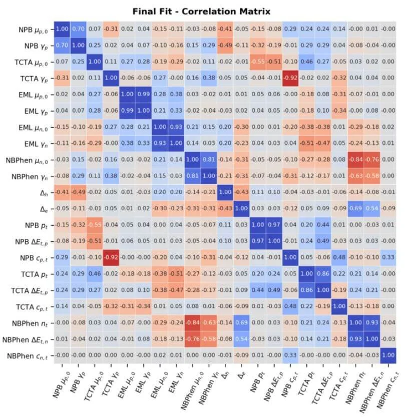
Figure 10. Correlation matrix of the final fit shown in Figure 8. Only the correlations among the parameters that were used to fit the experimental curves are calculated. The measurement techniques that are considered are IV between -1 to 6 V, C-f and G-f at offset voltages 1, 2 and 3 V, injection-CELIV at V = 3 V as well as TEL rise at 7 V.
A second criterion to assess the reliability of the extracted parameters is the sensitivity of the investigated characterization techniques to the material parameters. Parameter sensitivity analysis can be divided into a local and a global one. The first evaluates the influence of a parameter variation around a specific local working point on the agreement between simulation and measurement. Here, the sensitivity is evaluated for the final fitting parameters as working point, yielding the sensitivity of the final fit (Figure 8) on each of the parameters.
Global sensitivity analyzes the combined effect of varying all parameters within a certain range. These randomized simulation results are typically shown as scatter plots. 76 While it can give more general insights into the sensitivity of specific measurement techniques to material parameters, it is more difficult to be quantified compared to the local sensitivity analysis and computationally more demanding. In the scope of this tutorial we therefore focus on the local parameter sensitivity at the final fit.
In previous publications on single-carrier devices and on organic as well as perovskite solar cells we have studied the qualitative influence of the involved parameters by a systematic variation around the values from the final fit. 19,27,60 In the present paper on OLEDs we show the sensitivity of the electron mobility parameters µ0,e and γe of the EML as well as the zero-field hole mobility in the NBPhen layer on the selected measurements (Figure S9). Due to the large number of parameters, devices and performed measurements this will not be presented here in detail. Both EML parameters show a certain influence on one or the other experiment. Interestingly, they seem not to influence the TEL rise (Figure S9 (e, k)) while both have for example an effect on the IV curve between 2 and 3 V (Figure S9 (a, f)). Therefore these parameters cannot be accurately determined from a TEL rise fit alone. This finding again demonstrates how important it is to combine different measurement to be sensitive to as many parameters as possible. In Figure S9 we also show a parameter sweep of the NBPhen hole mobility. Note that this parameter was not used as a fitting parameter. A variation of ± one order of magnitude does not have any influence on the selected measurement techniques. One can say that we are not sensitive to this parameter and one should thus not try to determine this parameter from the selected experiments.
In order to obtain a more quantitative analysis of the sensitivity with respect to the involved model parameters, we again consider the error fi between the measured data and the simulation at N different user-defined target points (see equation (5)) and define the local sensitivity as

The calculated local sensitivity can take values between zero and infinity. The results are shown in Figure 11 and ordered from high to low. There is no general definition of a value that is still acceptable. In order to simplify the intepretation of the calculated local sensitivity, three groups of “high”, “medium” and “low” sensitivity were defined according to the observations in the parameter sweeps (Figure S9). In the following discussion we will show three examples (marked in blue in Figure 11) to illustrate the different sensitivities.
The hole (minority carrier) mobility in NBPhen is an example of “low” sensitivity. Such parameters cannot be determined accurately from the global fit. In this study, the minority carrier mobilities were not used as a fitting parameter. The field-enhancement coefficient of the EML electron mobility is a good example for “medium” sensitivity. It has some effect on some of the selected experiment but its influence is not that large. Parameters with a “high” sensitivity show a clear trend in the experiment when they are varied. Those parameters can safely be determined from the global fit, provided that they also show a low correlation to other parameters. Overall, we find that owing to the combination of 4 different experimental techniques and 8 different devices, the model is sensitive enough to all fitted parameters.

This tutorial has been published in the Journal of Applied Physics by S. Jenatsch and colleagues. All input and fit parameters required to perform the simulation and check for the quality of the fitting are reported in TABLE 1 of this paper.
This work has been supported financially by the European projects MOSTOPHOS (Grant Agreement Nos. 646259) and CORNET (Grant Agreement Nos. 760949).
2 P. T. Kissinger and W. R. Heineman, J. Chem. Educ. 60, 9242 (1983). https://doi.org/10.1002/anie.201004874,
3 A. J. Bard and L. R. Faulkner, Electrochemical Methods, 2nd ed. (John Wiley & Sons, Inc. , 2001).
4 J. Sworakowski and K. Janus, Org. Electron. Phys. Mater. Appl. 48, 46 (2017). https://doi.org/10.1016/j.orgel.2017.05.031,
5 D. R. T. Zahn, G. N. Gavrila, and M. Gorgoi, Chem. Phys. 325, 99 (2006). https://doi.org/10.1016/j.chemphys.2006.02.003,
6 A. Salehi, Y. Chen, X. Fu, C. Peng, and F. So, ACS Appl. Mater. Interfaces 10(11), acsami.7b18514 (2018).
7 A. Mikaeili, T. Matsushima, Y. Esaki, S. A. Yazdani, C. Adachi, and E. Mohajerani, Opt. Mater. 91, 93 (2019). https://doi.org/10.1016/j.optmat.2019.03.012,
8 T. Matsushima, K. Shiomura, S. Naka, and H. Murata, Thin Solid Films 520, 2283 (2012). https://doi.org/10.1016/j.tsf.2011.09.060
9 Y. Esaki, T. Komino, T. Matsushima, and C. Adachi, J. Phys. Chem. Lett. 8, 5891 (2017).https://doi.org/10.1021/acs.jpclett.7b02808
10 D. Yokoyama, A. Sakaguchi, M. Suzuki, and C. Adachi, Org. Electron. Phys. Mater. Appl. 10, 127 (2009). https://doi.org/10.1016/j.orgel.2008.10.010
11 M. T. Neukom, N. A. Reinke, K. A. Brossi, and B. Ruhstaller, Proc. SPIE 7722, 77220V (2010).
12 J. C. Blakesley, F. A. Castro, W. Kylberg, G. F. A. Dibb, C. Arantes, R. Valaski, M. Cremona, J. S. Kim, and J.-S. Kim, Org. Electron. 15, 1263 (2014). https://doi.org/10.1016/j.orgel.2014.02.008
13 M. T. Neukom, N. A. Reinke, and B. Ruhstaller, Sol. Energy 85, 1250 (2011). https://doi.org/10.1016/j.solener.2011.02.028
14 J. Staudigel, M. Stößel, F. Steuber, and J. Simmerer, J. Appl. Phys. 86, 3895 (1999). https://doi.org/10.1063/1.371306
15 M. Schober, M. Anderson, M. Thomschke, J. Widmer, M. Furno, R. Scholz, B. Lüssem, and K. Leo, Phys. Rev. B Condens. Matter Mater. Phys. 84, 165326 (2011). https://doi.org/10.1103/PhysRevB.84.165326
16 M. Mesta, M. Carvelli, R. J. De Vries, H. Van Eersel, J. J. M. Van Der Holst, M. Schober, M. Furno, B. Lüssem, K. Leo, P. Loebl, R. Coehoorn, and P. A. Bobbert, Nat. Mater. 12, 652 (2013). https://doi.org/10.1038/nmat3622
17 M. Neukom, S. Züfle, S. Jenatsch, and B. Ruhstaller, Sci. Technol. Adv. Mater. 19, 291 (2018). https://doi.org/10.1080/14686996.2018.1442091
18 M. T. Neukom, S. Züfle, and B. Ruhstaller, Org. Electron. 13, 2910 (2012). https://doi.org/10.1016/j.orgel.2012.09.008
19 S. Jenatsch, S. Altazin, P.-A. Will, M. T. Neukom, E. Knapp, S. Züfle, S. Lenk, S. Reineke, and B. Ruhstaller, J. Appl. Phys. 124, 105501 (2018). https://doi.org/10.1063/1.5044494 ,
20 M. Regnat, K. P. Pernstich, and B. Ruhstaller, Org. Electron. 70, 219 (2019). https://doi.org/10.1016/j.orgel.2019.04.027
21 S. Altazin, S. Züfle, E. Knapp, C. Kirsch, T. D. Schmidt, L. Jäger, Y. Noguchi, W. Brütting, and B. Ruhstaller, Org. Electron. 39, 244 (2016). https://doi.org/10.1016/j.orgel.2016.10.014
22 C. Peng, A. Salehi, Y. Chen, M. Danz, G. Liaptsis, and F. So, ACS Appl. Mater. Interfaces 9, 41421 (2017). https://doi.org/10.1021/acsami.7b13537
23 Fluxim AG, Switzerland, see www.fluxim.com for Platform for all-in-one characterization (Paios).
24 A. Salehi, C. Dong, D. H. Shin, L. Zhu, C. Papa, A. Thy Bui, F. N. Castellano, and F. So, Nat. Commun. 10, 2305 (2019). https://doi.org/10.1038/s41467-019-10260-7
25 S. L. M. Van Mensfoort and R. Coehoorn, Phys. Rev. Lett. 100, 1 (2008). https://doi.org/10.1103/PhysRevLett.100.086802
26 S. Jenatsch, R. Hany, A. C. Véron, M. Neukom, S. Züfle, A. Borgschulte, B. Ruhstaller, and F. Nüesch, J. Phys. Chem. C 118, 17036 (2014). https://doi.org/10.1021/jp5005314
27 M. T. Neukom, A. Schiller, S. Züfle, E. Knapp, J. Ávila, D. Pérez-del-Rey, C. Dreessen, K. P. S. Zanoni, M. Sessolo, H. J. Bolink, and B. Ruhstaller, ACS Appl. Mater. Interfaces 11, 23320 (2019). https://doi.org/10.1021/acsami.9b04991
28 G. Garcia-Belmonte, A. Guerrero, and J. Bisquert, J. Phys. Chem. Lett. 4, 877 (2013). https://doi.org/10.1021/jz302064z
29 S. Nowy, W. Ren, A. Elschner, W. Lövenich, and W. Brütting, J. Appl. Phys. 107, 054501 (2010). https://doi.org/10.1063/1.3294642 ,
30 S. Züfle, S. Altazin, A. Hofmann, L. Jäger, M. T. Neukom, W. Brütting, and B. Ruhstaller, J. Appl. Phys. 122, 115502 (2017). https://doi.org/10.1063/1.4992041 ,
31 E. Knapp and B. Ruhstaller, J. Appl. Phys. 112, 024519 (2012). https://doi.org/10.1063/1.4739303 ,
32 S. Nowy, W. Ren, J. Wagner, J. A. Weber, and W. Brütting, Proc. SPIE 7415, 74150G (2009). https://doi.org/10.1117/12.824856
33 E. Knapp and B. Ruhstaller, Appl. Phys. Lett. 99, 093304 (2011). https://doi.org/10.1063/1.3633109 ,
34 F. Fabregat-Santiago, G. Garcia-Belmonte, I. Mora-Sero, and J. Bisquert, Phys. Chem. Chem. Phys. 13, 9083 (2011). https://doi.org/10.1039/c0cp02249g
35 I. Mora-Seró, G. Garcia-Belmonte, P. P. Boix, M. A. Vázquez, and J. Bisquert, Energy Environ. Sci. 2, 678 (2009). https://doi.org/10.1039/b812468j
36 D. J. Pinner, R. H. Friend, and N. Tessler, J. Appl. Phys. 86, 5116 (1999). https://doi.org/10.1063/1.371488 ,
37 S. Barth, P. Müller, H. Riel, P. F. Seidler, W. Rieß, H. Vestweber, and H. Bässler, J. Appl. Phys. 89, 3711 (2001). https://doi.org/10.1063/1.1330766 ,
38 B. Ruhstaller, S. A. Carter, S. Barth, H. Riel, W. Riess, and J. C. Scott, J. Appl. Phys. 89, 4575 (2001). https://doi.org/10.1063/1.1352027 ,
39 Q. Niu, P. W. M. Blom, F. May, P. Heimel, M. Zhang, C. Eickhoff, U. Heinemeyer, C. Lennartz, and N. I. Crăciun, J. Appl. Phys. 122, 185502 (2017). https://doi.org/10.1063/1.5006587 ,
40 B. Ruhstaller, T. Beierlein, H. Riel, S. Karg, J. C. Scott, and W. Riess, IEEE J. Sel. Top. Quantum Electron. 9, 723 (2003). https://doi.org/10.1109/JSTQE.2003.818852
41 S. Wehrmeister, L. Jäger, T. Wehlus, A. F. Rausch, T. C. G. Reusch, T. D. Schmidt, and W. Brütting, Phys. Rev. Appl. 3, 024008 (2015). https://doi.org/10.1103/PhysRevApplied.3.024008
42 S. Mladenovski, S. Hofmann, S. Reineke, L. Penninck, T. Verschueren, and K. Neyts, J. Appl. Phys. 109, 083114 (2011). https://doi.org/10.1063/1.3576114 ,
43 M. Regnat, K. P. Pernstich, K.-H. Kim, J.-J. Kim, F. Nüesch, and B. Ruhstaller, “Routes for efficiency enhancement in fluorescent TADF Exciplex host OLEDs gained from an electro-optical device model ,” Adv. Electron. Mater. (2019). https://doi.org/10.1002/aelm.201900804
44 T. D. Schmidt, L. Jäger, Y. Noguchi, H. Ishii, and W. Brütting, J. Appl. Phys. 117, 215502 (2015). https://doi.org/10.1063/1.4921829 ,
45 G. Juška, M. Viliūnas, K. Arlauskas, N. Nekrašas, N. Wyrsch, and L. Feitknecht, J. Appl. Phys. 89, 4971 (2001). https://doi.org/10.1063/1.1359436 ,
46 G. Juška, K. Arlauskas, M. Viliūnas, and J. Kočka, Phys. Rev. Lett. 84, 4946 (2000). https://doi.org/10.1103/PhysRevLett.84.4946
47 V. Kažukauskas, A. Arlauskas, M. Pranaitis, R. Lessmann, M. Riede, and K. Leo, Opt. Mater. (Amsterdam) 32, 1676 (2010). https://doi.org/10.1016/j.optmat.2010.04.008
48 L. Wang, S. Jenatsch, B. Ruhstaller, C. Hinderling, D. Gesevičius, R. Hany, and F. Nüesch, Adv. Funct. Mater. 28, 1705724 (2018). https://doi.org/10.1002/adfm.201705724
49 S. Züfle, S. Altazin, A. Hofmann, L. Jäger, M. T. Neukom, T. D. Schmidt, W. Brütting, and B. Ruhstaller, J. Appl. Phys. 121, 175501 (2017). https://doi.org/10.1063/1.4982903 ,
50 Y. Gao, A. Pivrikas, B. Xu, Y. Liu, W. Xu, P. H. M. Van Loosdrecht, and W. Tian, Synth. Met. 203, 187 (2015). https://doi.org/10.1016/j.synthmet.2015.02.036
51 O. J. Sandberg, M. Nyman, S. Dahlström, S. Sandén, B. Törngren, J. H. Smått, and R. Österbacka, Appl. Phys. Lett. 110, 153504 (2017). https://doi.org/10.1063/1.4980101 ,
52 O. J. Sandberg and M. Nyman, Org. Electron. Phys. Mater. Appl. 64, 97 (2019). https://doi.org/10.1016/j.orgel.2018.10.017
53 A. J. Mozer, N. S. Sariciftci, L. Lutsen, D. Vanderzande, R. Österbacka, M. Westerling, and G. Juška, Appl. Phys. Lett. 86, 112104 (2005). https://doi.org/10.1063/1.1882753 ,
54 S. Bange, M. Schubert, and D. Neher, Phys. Rev. B: Condens. Matter Mater. Phys. 81, 035209 (2010). https://doi.org/10.1103/PhysRevB.81.035209
55 J. Lorrmann, B. H. Badada, O. Inganäs, V. Dyakonov, and C. Deibel, J. Appl. Phys. 108, 113705 (2010). https://doi.org/10.1063/1.3516392 ,
56 A. Armin, G. Juska, M. Ullah, M. Velusamy, P. L. Burn, P. Meredith, and A. Pivrikas, Adv. Energy Mater. 4, 1300954 (2014). https://doi.org/10.1002/aenm.201300954
57 B. Ruhstaller, E. Knapp, B. Perucco, N. Reinke, D. Rezzonico, and F. Müller, in Optoelectronic Devices and Properties, edited by P. O. Sergiyenko (InTech , 2011).
58 S. Altazin, L. Penninck, and B. Ruhstaller, Handbook of Organic Light-Emitting Diodes (Springer Japan , Tokyo , 2018), pp. 1–22 .
59 Fluxim AG, Switzerland, see www.fluxim.com for Simulation software Setfos (version 4.6).
60 R. Häusermann, E. Knapp, M. Moos, N. A. Reinke, T. Flatz, and B. Ruhstaller, J. Appl. Phys. 106, 104507 (2009). https://doi.org/10.1063/1.3259367 ,
61 H. Shin, J.-H. Lee, C.-K. Moon, J.-S. Huh, B. Sim, and J.-J. Kim, in Org. Light Emit. Mater. Devices XX, edited by F. So, C. Adachi, and J.-J. Kim (International Society for Optics and Photonics, 2016), p. 99411X. https://doi.org/10.1117/12.2236763
62 A. Salehi, S. Ho, Y. Chen, C. Peng, H. Yersin, and F. So, Adv. Opt. Mater. 5, 1700197 (2017). https://doi.org/10.1002/adom.201700197
63 H. Nakanotani, K. Masui, J. Nishide, T. Shibata, and C. Adachi, Sci. Rep. 3, 2127 (2013). https://doi.org/10.1038/srep02127
64 D.-S. Leem, S. O. Jung, S.-O. Kim, J.-W. Park, J. W. Kim, Y.-S. Park, Y.-H. Kim, S.-K. Kwon, and J.-J. Kim, J. Mater. Chem. 19, 8824 (2009). https://doi.org/10.1039/b915384e
65 M. Regnat, K. P. Pernstich, S. Züfle, and B. Ruhstaller, ACS Appl. Mater. Interfaces 10, 31552 (2018). https://doi.org/10.1021/acsami.8b09595
66 S. Gottardi, M. Barbry, R. Coehoorn, and H. Van Eersel, Appl. Phys. Lett. 073301, 1 (2018). https://doi.org/10.1063/1.5079642
67 H. Yoshida and K. Yoshizaki, Org. Electron. Phys. Mater. Appl. 20, 24 (2015). https://doi.org/10.1016/j.orgel.2015.01.037
68 T.-Y. Chu and O.-K. Song, Appl. Phys. Lett. 90, 203512 (2007). https://doi.org/10.1063/1.2741055 ,
69 N. B. Kotadiya, H. Lu, A. Mondal, Y. Ie, D. Andrienko, P. M. W. M. W. Blom, and G.-J. A. H. A. Wetzelaer, Nat. Mater. 17, 329 (2018). https://doi.org/10.1038/s41563-018-0022-8
70 J. Li, S. C. Dong, A. Opitz, L. S. Liao, and N. Koch, J. Mater. Chem. C 5, 6989 (2017). https://doi.org/10.1039/C7TC02248D
71 S. Naka, H. Okada, H. Onnagawa, and T. Tsutsui, Appl. Phys. Lett. 76, 197 (2000). https://doi.org/10.1063/1.125701 ,
72 S. L. M. van Mensfoort and R. Coehoorn, Phys. Rev. B 78, 085207 (2008). https://doi.org/10.1103/PhysRevB.78.085207
73 E. Knapp, R. Häusermann, H. U. Schwarzenbach, and B. Ruhstaller, J. Appl. Phys. 108, 054504 (2010). https://doi.org/10.1063/1.3475505 ,
74 A. S. D. Sandanayaka, T. Matsushima, and C. Adachi, J. Phys. Chem. C 119, 23845 (2015). https://doi.org/10.1021/acs.jpcc.5b07084
75 J. S. Bangsund, K. W. Hershey, and R. J. Holmes, ACS Appl. Mater. Interfaces 10, 5693 (2018). https://doi.org/10.1021/acsami.7b16643
76 S. Jenatsch, S. Züfle, P.-A. Will, B. Blülle, M. Neukom, S. Lenk, S. Reineke, D. Braga, K. Domanski, and B. Ruhstaller, SID Symp. Dig. Tech. Pap. 50, 1895 (2019). https://doi.org/10.1002/sdtp.13333