Quantifying Electro-Optical Cross-Talk in White OLED / Color Filter Displays
Here, we show how the simulation software Laoss can be used to quantitatively analyze optical and electrical cross-talk effects in white organic light-emitting diode (WOLED) / color filter (CF) displays. Optical light leakage is found to be highly influenced by the topography of the pixel definition layer (PDL) while it only shows little correlation with OLED parameters, such as the emitter orientation. Electro-optical simulations exemplify the importance of electrical and optical cross-talk to be dominant in different voltage ranges.
1. Introduction
A considerable number of smartphone and television displays are nowadays made of OLEDs due to their high level of sharpness, contrast ratio, and stunning color gamut. Basically, there are two different ways in how the primary colors are generated. Either they are directly generated by using blue, green, and red OLEDs, or the light of a common white OLED is filtered by selective color filters. The RGB approach is typically energy-efficient but requires precise engineering work during fabrication. Because of the higher defect tolerance, the WOLED/CF approach is often used for large-area applications, such as television screens.
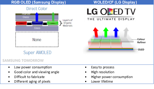
Table 1: comparison of direct emission RGB OLED with WOLED/CF displays. https://news.samsung.com/global/galaxy-tab-s-explained-super-amoled-display; https://www.cnet.com/news/phone-oled-vs-tv-oled-whats-the-difference/
Common to both technologies is that increasing the pixel density and brightness requires the pixels to be close to each other. Besides being a complex fabrication process, this can be a technological challenge also for the rise of the pixel cross-talk, i.e., the electrical or optical coupling between adjacent pixels in the matrix. The electrical cross-talk is caused by lateral current flow through common layers,[1,2] whereas the optical cross-talk is due to light leakage through non-addressed pixels. Pixel cross-talk reduces the contrast ratio and hampers the color gamut of the final display. Therefore, understanding and reducing pixel cross-talk effects are of great importance for future display designs.
In WOLED/CF displays both electrical and optical cross-talk effects can occur and their interplay might become important as well. In order to understand their origin and optimize the material and layouts of displays, the use of simulation software is highly desirable.
We first focus solely on optical cross-talk and analyze the effect of different display parameters, such as OLED – filter distance or pixel definition shape, on the cross-talk parameters. In a second step, we also consider electrical cross-talk between the individual WOLED pixels and investigate the effect on emitted color after the CF display. Combining both electrical and optical cross-talk for a single device layout demonstrates that at a luminance of 1000 cd/m^2 both effects contribute roughly equally while for lower (higher) voltages the electrical (optical) contribution dominates.
Our results demonstrate that numerical simulations can capture the nature of pixel cross-talk in OLED arrays. Such simulations are thus a suitable tool to optimize the characteristics of the pixel matrix without costly and time-consuming processes of device fabrication and testing.
2. Methods
The optical simulation of a WOLED/CF display is performed in the commercial software Laoss.[3] The model is based on a 3D ray-tracing algorithm. In Laoss, the display is represented by two interfaces (OLED and CF plane) separated by a certain distance d. Inputs are the lateral dimensions and topography of OLED and CF planes as well as the thickness and refractive index of the material in between (called encapsulation layer). The layout for the WOLED/CF was previously analyzed by Lee et al. using simulations based on a finite-difference time-domain method.[4] For simplicity, we neglect the topography of the filter plane and only consider a real and constant refractive index for the encapsulation layer. Further inputs are the angle-dependent optical properties of the WOLED and the CFs. Those were simulated using the software Setfos.[3] The necessary input data was taken from a publication by Chang et al.[5] as well as the Setfos refractive index database. The electrical simulation is based on a 2+1D finite element method (FEM) implemented in Laoss. Laoss solves the current continuity equation through the FEM in 2D domains, i.e. the top and bottom electrodes of the WOLED. The two domains are coupled via a “coupling law” given by the current density-voltage (J-V) characteristics of the pixel. For the structure employed in this study, the J-V coupling law is extracted from the experimental data previously reported.[5] For all the simulations we address the OLED below the green color filter. We directly analyze the emitted intensity above the CF interface displayed in the Laoss software. In order to quantify the cross-talk, we define the cross-talk indices defined as the integrated intensity of the adjacent pixel, e.g. white, divided by the integrated radiant intensity R above the addressed pixel, i.e. green.

Moreover, we can analyze the emission integrated over all x and y dimensions. This is used to determine the emitted color of the display in forward direction.
This simulation has been carried on with LAOSS. If you want more information, check the LAOSS main page
3. Results
Optical Pixel Cross-Talk: The layout of the CF and WOLED layer is shown in Figure 1. One repeating pixel unit consists of red, green, blue, and white pixels which all have the same dimensions. The size of this repeating unit corresponds approximately to a display resolution of 300 PPI. To reproduce the extended 2D structure in a real display within our simulation, we use periodic boundary conditions, i.e. we assume that every ray that exits the stack on the side is entering on the opposite side. The unit and pixel dimensions are kept constant for all the simulations.
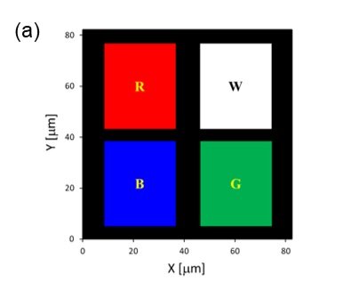

Figure 1. Layout of the CF (a) and WOLED (b) plane used in the optical simulation. The CF and WOLED planes are separated by the encapsulation layer with thickness d.
The parameters that are varied in the following optical simulations are (the base case settings are listed in brackets)
• The distance d between the WOLED and CF plane (d = 3.6 µm)
• The angle β of the PDL structure (β = 45°)
• The refractive index n of the encapsulation material (n = 1.5)
The intensity map above the four pixels for the base case simulation is shown in Figure 2(a). The edges of the four pixels are indicated as guidance. The highest intensity can be observed for the green pixel which is the one that is being addressed. Some light leakage is also observed for the white pixel above, predominantly at the edge of the pixel. This feature is specific for optical cross-talk in contrast to electrical cross-talk which results in homogeneous lighting up of adjacent pixels. [1,2] The cross-talk to the red and the blue pixels are much lower due to (a) the larger distance to the green pixel and (b) the color filters which block a certain wavelength range, reducing the integrated intensity.
Starting from this base case we now varied the distance between WOLED and CF plane as well as the steepness of the PDL structure. On the one hand, increasing the thickness of the encapsulation layer results in a clear increase in the cross-talk index Cwg (Figure 2(b)). This is not really a surprising result. On the other hand, the angle of the PDL structure has a rather unexpected effect on the white cross-talk index Cwg. Interestingly, a slope of 0°, i.e. no PDL structure, results in almost no cross-talk for small values of d. For steeper PDLs up to about 60°, the cross-talk effect increases to several percent, while it decreases again for steeper walls. Typical PDL structures feature an angle of 30° - 45°. [6,7] This demonstrates that there could be some optimization potential in this direction to reduce cross-talk.

Figure 2. (a) Simulated intensity map of one simulation unit with indicated positions of red, blue, white and green pixels. (b) white cross-talk index as a function of encapsulation layer thickness and PDL slope.
All the other cross-talk indices are showing a similar trend with distance and PDL slope but are at least one order of magnitude lower. This is clear as the intensity of the light that is leaking through the blue and red filters is further reduced because of the color filters. The effect of further display parameters could be analyzed in a similar way. Here we want to turn our attention to a further OLED parameter which is commonly tuned for more efficient OLEDs. This parameter is the emitter orientation which can be determined using our measurement instrument Phelos. In the Laoss simulation, we compare the cross-talk effect of isotropically oriented emitters with perfectly horizontal emitters in the WOLED. The intensity maps for these two situations are shown in Figure 3. It can easily be seen that the absolute intensity of the green pixel is considerably higher for horizontal emitter orientation which is expected. Interestingly, the cross-talk index Cwg is only slightly reduced from 6.0% to 5.7% when the emitters in the WOLED are arranged perfectly horizontal. A similar result has been obtained by Lee et al. [4]

Figure 3. The X/Y intensity map of (a) isotropic and (b) horizontal dipole orientation.
Electro-Optical Pixel Cross-Talk: In order to compare the electrical and optical contribution of the cross-talk in a WOLED/CF display, the base case simulation from the previous section is used and extended with the Laoss electrical simulation.[3] The required sheet resistance values and the IV curve of the white OLED are taken from previous publications.[1,5] Electrical and optical cross-talk indices are evaluated as a function of the applied voltage to the green pixel (see Figure 4 (a)). At voltages right above turn-on, the Cwg value arises to about 10% and decreases steadily for increasing voltage. This value is in close agreement with previous reports.[1,2] When we disentangle both contributions we can see that the optical cross-talk shows no voltage dependence and stays at a constant value of about 0.7%. This is expected from a light leakage effect as both the addressed and the adjacent pixel’s intensity would be scaled with the same factor. The strong voltage dependence can thus be solely attributed to the electrical cross-talk. Moreover, there is a crossing point at about 7.5 V at which the optical contribution overtakes the electrical contribution. At high brightness values, which are used in real applications, the optical cross-talk is dominating the overall effect and countermeasures should therefore predominantly address the reduction of the optical cross-talk contribution. In Figure 4 (b) the far-field color (red points) of the display is shown as a function of voltage. The color gamut is clearly reduced at low driving voltages of 2.7V. As the cross-talk reduces quickly, the color point moves close to the theoretically achievable green color point defined by the chosen WOLED and green color filter.

Figure 4. (a) Electrical, optical and electro-optical cross-talk index as a function of OLED driving voltage. The luminance of the white pixel is shown as a reference. (b) Color coordinates of the primary colors (black and white circles) and far-field color point (red circles) with increasing voltage.
If you are interested in performing this simulation you can try LAOSS for 1 month
4. Conclusion
We simulated optical and electro-optical cross-talk in WOLED/CF displays with the commercial software Laoss. For a test structure with a typical layout, we demonstrated that our method can estimate the light leakage and give information about the expected modification of the display color gamut. Topography variations of the WOLED layer give insights into optimized PDL structures. Similarly, the refractive index of the material between WOLED and CF can be optimized to reduce optical cross-talk effects. Combining electrical and optical simulations allow us to investigate the overall cross-talk effect and evaluate the different contributions separately. We have shown the detrimental effect of electro-optical cross-talk on the color gamut of the display as a function of the applied voltage.
Together, the presented results demonstrate that it is possible to describe and quantify cross-talk in OLED displays with numerical simulations and, eventually, minimizing these parasitic effects without the need of fabricating multiple test devices. Further studies could analyze the contribution of CF topography, increasing pixel density, or varied OLED arrangements in order to minimize cross-talk and explore the full-color gamut of the display.
5. References
1. Diethelm M, Penninck L., Altazin S., Hiestand R., Kirsch C., Ruhstaller B. Quantitative analysis of pixel crosstalk in AMOLED displays, J. Inf. Display 19, 61, (2018)
2. L. Penninck, M. Diethelm, S. Altazin, R. Hiestand, C. Kirsch, B. Ruhstaller, Modelling crosstalk through common semiconductor layers in AMOLED displays, J. Soc. Inf. Display 26, 546, (2018)
3. Laoss and Setfos simulation software by Fluxim AG
4. Lee J. K., Cho S., Kang D. W., Analysis of light leakage between the adjacent pixels in a color-filter stacked white OLED display, Displays 45, 6, (2016).
5. Chang C.-H., et al., Enhancing color gamut of white OLED displays by using microcavity green pixels, Organic Electronics 11, 247-254 (2010).
6. Lee W.-K. et al., Three-dimensional pixel configurations for optical outcoupling of OLED displays—optical simulation, J. Inf. Display 27, 5, (2019) 7. Kang K., Yoon J., Kim J., Lee H., Yang B. Effect of the finite pixel boundary on the angular emission characteristics of top-emitting organic light-emitting diodes, Optics Express 23, 11, (2015)